Adhesive tape for semiconductor wafer processing and method for processing semiconductor wafer
A technology of wafer processing and processing method, which is applied in the field of tapes for semiconductor wafer processing, can solve the problems of adhesive residue, leakage, residual glue, etc., and achieve the effect of excellent relaxation
- Summary
- Abstract
- Description
- Claims
- Application Information
AI Technical Summary
Problems solved by technology
Method used
Image
Examples
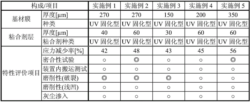
Embodiment 1
[0113] An acrylic copolymer composed of 2-ethylhexyl acrylate (78mol%), 2-hydroxyethyl acrylate (21mol%), and methacrylic acid (1mol%) was prepared, after which the acrylic acid The hydroxyl group in the repeating unit obtained from 2-hydroxyethyl ester reacts with 2-(methacryloyloxy)ethyl isocyanate to obtain a carbon-carbon double bond that is radiation-curable on the side chain of the polymer. Functional methacryloyl acrylic copolymer. In the obtained acrylic copolymer, a trifunctional ultraviolet curing type urethane acrylate oligomer (manufactured by Nippon Synthetic Chemicals Co., Ltd., (trade name) Violet 75 parts by mass of UV-7550B) and 5.0 parts by mass of a photopolymerization initiator ((trade name), manufactured by BASF JAPAN Co., Ltd., Irgacure 184) to obtain an adhesive composition.
[0114] Apply the following adhesive a mainly composed of (meth)acrylic copolymer on a 25 μm polyethylene terephthalate (PET) spacer, and dry it at 120°C for 2 minutes to set the t...
Embodiment 2
[0117] The above-mentioned adhesive a was coated on a 25 μm polyethylene terephthalate spacer, dried at 120°C for 2 minutes to form an adhesive layer with a thickness of 60 μm, and the adhesive layer was bonded to A tape for semiconductor wafer processing was produced on a substrate film made of the above-mentioned urethane acrylate having a thickness of 270 μm.
Embodiment 3
[0119] The above-mentioned adhesive a was coated on a 25 μm polyethylene terephthalate spacer, dried at 120°C for 2 minutes to form an adhesive layer with a thickness of 60 μm, and the adhesive layer was bonded to A tape for semiconductor wafer processing was produced on a substrate film made of the above-mentioned urethane acrylate having a thickness of 100 μm.
PUM
| Property | Measurement | Unit |
|---|---|---|
| height | aaaaa | aaaaa |
| height | aaaaa | aaaaa |
| thickness | aaaaa | aaaaa |
Abstract
Description
Claims
Application Information


