Mold release film, method for manufacturing same, and method for manufacturing semiconductor package

A manufacturing method and release film technology, applied in semiconductor/solid-state device manufacturing, semiconductor devices, semiconductor/solid-state device components, etc., can solve problems such as easy electrification, semiconductor chip damage, etc. , Difficult to curl the effect of mold compliance

Active Publication Date: 2016-11-09
ASAHI GLASS CO LTD
View PDF12 Cites 5 Cited by
  • Summary
  • Abstract
  • Description
  • Claims
  • Application Information

AI Technical Summary

Problems solved by technology

At this time, if the release film is easily charged, there is a possibility that the semiconductor chip will be damaged due to charge-discharge during peeling.

Method used


Image

  • Mold release film, method for manufacturing same, and method for manufacturing semiconductor package
  • Mold release film, method for manufacturing same, and method for manufacturing semiconductor package
  • Mold release film, method for manufacturing same, and method for manufacturing semiconductor package

Examples


no. 1 Embodiment approach

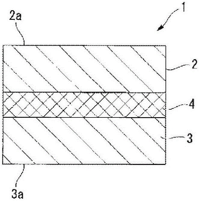
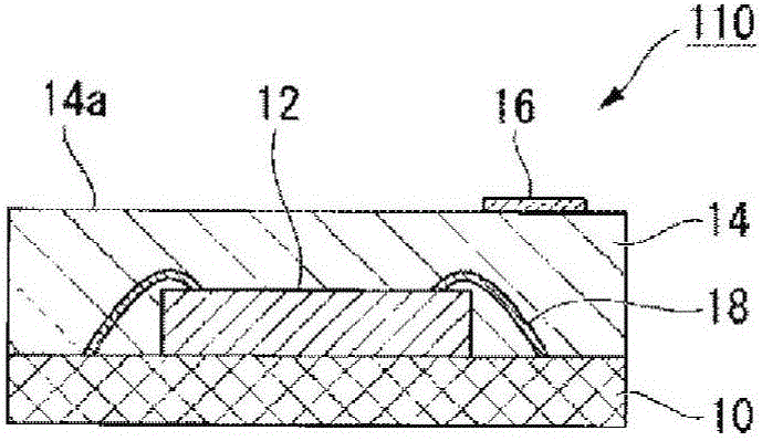
[0277] As an embodiment of the manufacturing method of a semiconductor package, it is directed to using the above-mentioned release film 1 as a release film and manufacturing it by compression molding. figure 2 The illustrated situation of the semiconductor package 110 is described in detail. The manufacturing method of the semiconductor package of this embodiment has the following process (α1)-(α7).

[0278] (α1) The release film 1 is arranged so that the release film 1 covers the cavity of the mold and the surface 2a of the release film 1 on the first thermoplastic resin layer 2 side faces the space in the cavity (the second thermoplastic resin layer 3 side The surface 3a faces the cavity surface) process.

[0279] (α2) A step of vacuum-adsorbing the release film 1 to the cavity surface side of the mold.

[0280] (α3) A step of filling the cavity with a curable resin.

[0281] (α4) Arranging the substrate 10 mounted with a plurality of semiconductor chips 12 at predeterm...

no. 2 Embodiment approach

[0321] As another embodiment of the manufacturing method of the semiconductor package, for using the above-mentioned release film 1 as the release film, it is manufactured by the transfer molding method. figure 2 The illustrated situation of the semiconductor package 110 is described in detail.

[0322] The manufacturing method of the semiconductor package of this embodiment has the following process (β1)-(β7).

[0323] (β1) The release film 1 is arranged so that the release film 1 covers the cavity of the mold and the surface 2a of the release film 1 on the first thermoplastic resin layer 2 side faces the space in the cavity (the second thermoplastic resin layer 3 side) The surface 3a faces the cavity surface) process.

[0324] (β2) A step of vacuum-adsorbing the release film 1 to the cavity surface side of the mold.

[0325] (β3) A step of disposing the substrate 10 on which the plurality of semiconductor chips 12 are mounted at predetermined positions in the cavity.

[...

no. 3 Embodiment approach

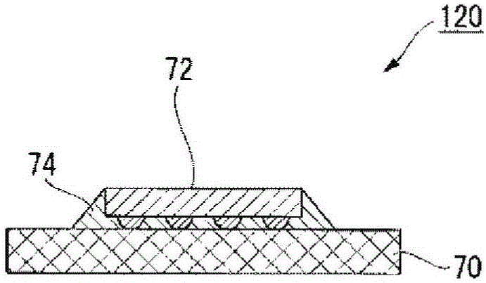
[0351] As another embodiment of the manufacturing method of the semiconductor package, for using the above-mentioned release film 1 as the release film, it is manufactured by the transfer molding method. image 3 The illustrated situation of the semiconductor package 120 is described in detail.

[0352] The manufacturing method of the semiconductor package of this embodiment has the following process (γ1)-(γ5).

[0353] (γ1) The release film 1 is arranged such that the release film 1 covers the cavity of the upper mold of a mold having an upper mold and a lower mold and the surface 2a of the release film 1 on the first thermoplastic resin layer 2 side faces the mold. The process of creating a space in the cavity (the surface 3a on the side of the second thermoplastic resin layer 3 faces the cavity surface of the upper mold).

[0354] (γ2) A step of vacuum-adsorbing the release film 1 to the cavity surface side of the upper mold.

[0355] (γ3) Arrange the substrate 70 on whic...


PUM

PropertyMeasurementUnit
storage modulusaaaaaaaaaa
thicknessaaaaaaaaaa
peel strengthaaaaaaaaaa

Abstract

Provided are a mold release film, a method for manufacturing the same, and a method for manufacturing a semiconductor package using the mold release film. The mold release film is not easily charged and curled, does not contaminate a mold, and has excellent mold followability. In a method for manufacturing a semiconductor package in which a semiconductor element is arranged in a mold and the mold is sealed with a curable resin, thereby forming a resin-sealed portion, the mold release film is arranged on a surface with which the curable resin on the mold is in contact. The mold release film is provided with a first thermoplastic resin layer being in contact with the curable resin during the formation of the resin-sealed portion, a second thermoplastic resin layer being in contact with the mold during the formation of the resin-sealed portion, and an intermediate layer being arranged between the first thermoplastic resin layer and the second thermoplastic resin layer. The storage elastic moduli of the first thermoplastic resin layer and the second thermoplastic resin layer at 180 DEG C are respectively 10-300 MPa, the difference in the storage elastic modulus at 25 DEG C is 1,200 MPa or less, the thickness is 12-50 [mu]m, and the intermediate layer includes a polymeric antistatic agent.

Description

technical field [0001] The present invention relates to a release film arranged on the cavity surface of a mold in a method of manufacturing a semiconductor package in which a semiconductor element is arranged in a mold and sealed with a curable resin to form a resin sealing portion, a method for manufacturing the release film, and a method using the semiconductor element. The manufacturing method of the semiconductor package of the release film mentioned above. Background technique [0002] In order to block and protect the semiconductor chip from outside air, the semiconductor chip is usually sealed with a resin and mounted on a substrate as a molded product called a package. The sealing of the semiconductor chip is performed using curable resins such as thermosetting resins such as epoxy resins. As a method of sealing a semiconductor chip, for example, a method of arranging a substrate on which a semiconductor chip is mounted so that the semiconductor chip is located at ...

Claims


Application Information

Patent Timeline
Patent Type & Authority Applications(China)
IPC IPC(8): H01L21/56B29C33/68B29C43/18B29C45/14B32B27/00B32B27/18
CPCB29C43/18H01L21/566H01L2924/181H01L24/97H01L2224/16225H01L2224/32225H01L2224/48091H01L2224/73204B29C45/14655B29C45/02B29C2045/14663B32B27/18B32B7/12B32B27/06B32B27/16B32B27/34B32B27/36B32B2255/10B32B2264/102B32B2264/108B32B2307/21B32B2307/54B32B2307/732B29C33/68B32B27/08B32B27/322H01L2924/00012H01L2924/00014H01L2924/00B29K2627/18B29L2031/3481B32B37/12B32B2250/24B32B2327/18H01L23/293
Inventor 笠井涉铃木政己
Owner ASAHI GLASS CO LTD
Why Eureka
Try Eureka