Wafer flattening method

A flattening method and wafer technology, applied in gaseous chemical plating, decorative art, microstructure technology, etc., can solve problems such as wafer surface collapse, achieve the effects of reducing removal, controlling collapse, and increasing removal

Active Publication Date: 2016-11-16
BEIJING SEMICORE PRECISION MICROELECTRONICS EQUIP CO LTD
View PDF8 Cites 8 Cited by
  • Summary
  • Abstract
  • Description
  • Claims
  • Application Information

AI Technical Summary

Problems solved by technology

[0004] The purpose of the present invention is to provide a wafer planarization method to solve the problem of collapse on the wafer surface when the existing equipment technology is used to planarize large-scale graphic chips (such as micro-electromechanical system devices (MEMS)) question

Method used


Image

  • Wafer flattening method

Examples


Embodiment Construction

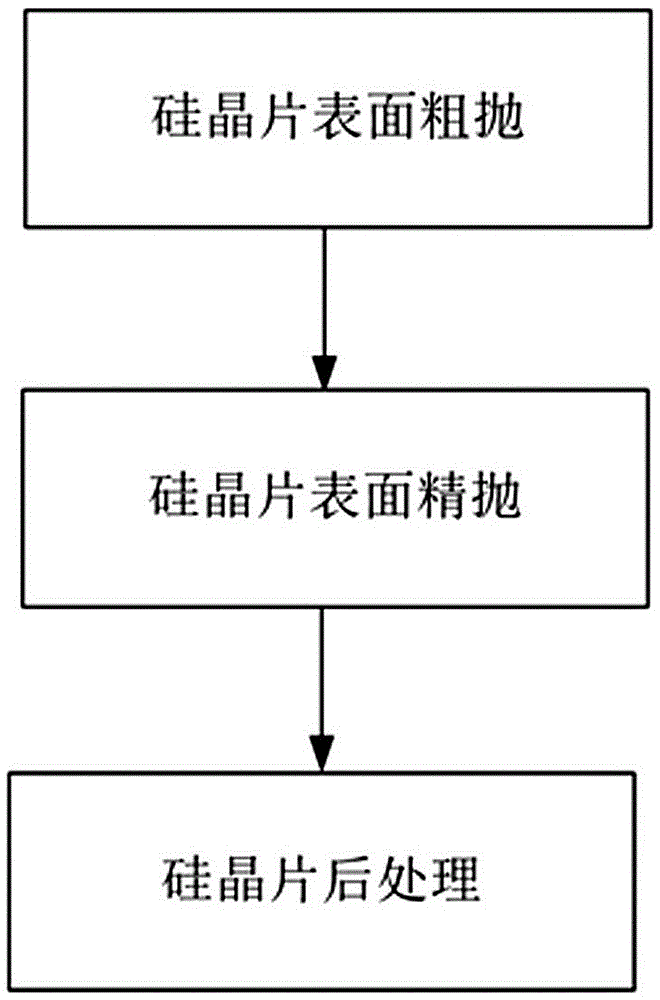
[0033] Hereinafter, embodiments of the wafer planarization method of the present invention will be described with reference to the accompanying drawings.

[0034] The examples described here are specific specific implementations of the present invention, and are used to illustrate the concept of the present invention. They are all explanatory and exemplary, and should not be construed as limiting the implementation of the present invention and the scope of the present invention. In addition to the embodiments described here, those skilled in the art can also adopt other obvious technical solutions based on the claims of the application and the contents disclosed in the description, and these technical solutions include adopting any obvious changes made to the embodiments described here. Replacement and modified technical solutions.

[0035] The accompanying drawings in this specification are schematic diagrams, which assist in explaining the concept of the present invention, a...


PUM

PropertyMeasurementUnit
particle diameteraaaaaaaaaa
compression ratioaaaaaaaaaa
hardnessaaaaaaaaaa

Abstract

The invention discloses a wafer flattening method. A wafer is a large-size graphics chip and comprises a wafer of a micro-electro-mechanical system (MEMS), and the thickness of the surface of the wafer is within 4 um to 10 um after filling oxides through chemical vapor deposition. The wafer flattening method comprises the following steps of step (1) rough polishing of the surface of the wafer: removing 75%-85% of oxides on the surface of the wafer through rough polishing; step (2) fine polishing of the surface of the wafer: utilizing a fixed abrasive polishing pad and polishing solution without abrasive to carry out fine polishing on the surface of the wafer which is subjected to rough polishing in the step (1) and removing residual oxides on the surface of the wafer; and step (3) wafer post-processing: utilizing deionized water to polish the surface of the wafer under the condition of low pressure, cleaning the residual polishing solution on the surface of the wafer and adjusting the surface of the wafer to hydrophobicity. The second step of the method is helpful for reducing the removal effect of the abrasive on the lower region while increasing the removal effect on the higher region, so that the collapse of the surface of the wafer is controlled.

Description

technical field [0001] The invention belongs to the technical field of semiconductor product processing, in particular to a wafer flattening method. Background technique [0002] It is usually used for wafer planarization of MEMS Micro-Electro-Mechanical System (MEMS Micro-Electro-Mechanical System) devices. Device technology presents challenges. In the CMP (Chemical Mechanica Polishing) process, the dishing control on the ultra-large line width of hundreds of microns is a very challenging topic. [0003] The reasons for the collapse are as follows: when dealing with a surface where multiple materials coexist, the surface collapse is caused by the different removal rates of the polishing fluid for different materials. For this type of collapse, it is fundamental to adjust the selection ratio of the polishing fluid to different materials , and at the same time rationally adjusting the ratio and balancing the removal time and rate of various materials will also play a role i...

Claims


Application Information

Patent Timeline
Patent Type & Authority Applications(China)
IPC IPC(8): B81C1/00
CPCB81C1/00206B81C1/00674
Inventor 李婷顾海洋
Owner BEIJING SEMICORE PRECISION MICROELECTRONICS EQUIP CO LTD
Why Eureka
Try Eureka