MEMS (micro-electro-mechanical system) chip with getters and wafer level packaging method thereof
A technology of MEMS structure layer and getter, which is applied in decorative art, electrical components, measuring devices, etc., can solve the problems of increasing MEMS chip area, low utilization rate of side, and inability to completely cover vertical side, so as to increase surface area, Guaranteed vacuum effect
- Summary
- Abstract
- Description
- Claims
- Application Information
AI Technical Summary
Problems solved by technology
Method used
Image

Examples
Embodiment 1
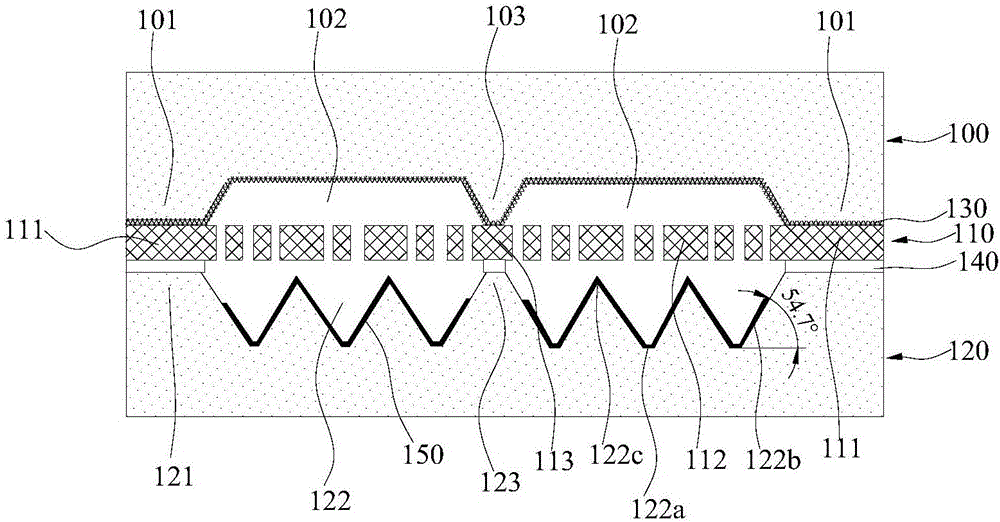
[0034] MEMS chips with getters such as image 3 As shown, it is composed of a cover plate 100, a MEMS structure layer 110 and a base plate 120. The cover plate 100 is formed with a cover plate sealing area 101, a cover plate bonding column 103 and two cover plate concave cavities 102, and their surfaces are formed with cover plates. Board insulating layer 130, its material is SiO 2 , the bottom of the cover cavity 102 is flat, and the side can be inclined or perpendicular to the bottom. The depth of the cover cavity 102 is generally 2-100 μm; through Si and SiO 2 The direct bonding process bonds a heavily doped Si wafer to the side of the cover plate 100 with a cavity, and then grinds it to the required thickness to form the MEMS structure layer 110. The MEMS structure layer 110 is divided into There are three parts: MEMS bonding area 111, MEMS structure 112 and MEMS bonding block 113; base plate sealing area 121, base plate bonding post 123 and two base plate cavities 122 ar...
Embodiment 2
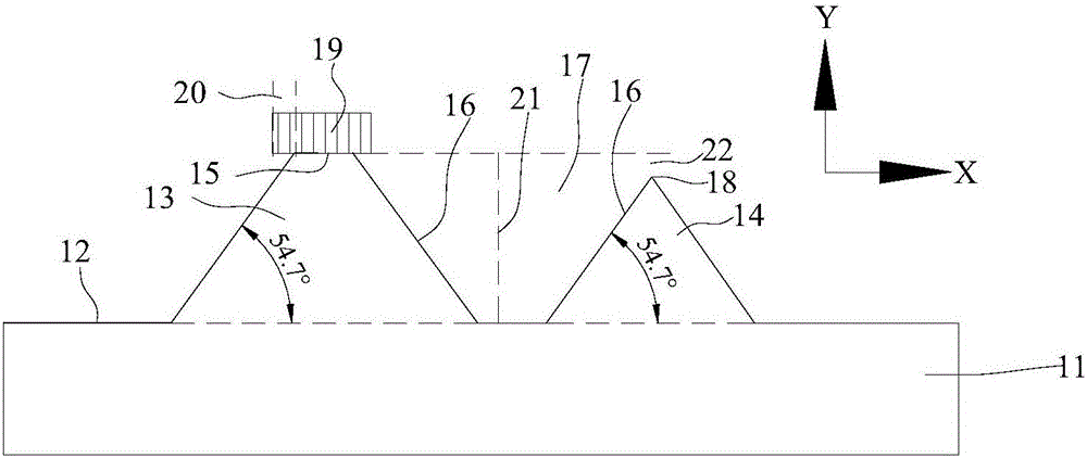
[0036] MEMS chips with getters such as Figure 4 As shown, it is composed of a cover plate 100, a MEMS structure layer 110 and a bottom plate 120. The cover plate 100 is made with a cover plate sealing area 101, a cover plate bonding column 103, a window 104 and two cover plate concave cavities 102; Inside the chamber 102, there are several prisms composed of slopes 102b, flat tops 102c, and bottoms 102a, and several pyramids composed of slopes 102b, pointed tops 102d, and bottoms 102a. The slopes 102b correspond to figure 2 The middle pyramid 14 and the inclined surface 16 of the truncated prism 13 correspond to the cover plate bonding post 103 and the flat top 102c figure 2 In the prism 13, the apex 102d corresponds to figure 2 In the pyramid 14, the height of the cover plate bonding post 103 is the same as that of the flat top 102c, the height of the pointed top 102d is smaller than the height of the flat top 102c, and the cover plate sealing area 101 and the surface of...
Embodiment 3
[0038] MEMS chips with getters such as Figure 5 As shown, it is composed of a cover plate 100, a MEMS structure layer 110 and a bottom plate 120. The cover plate 100 is made with a cover plate sealing area 101, a cover plate bonding column 103, a window 104 and two cover plate concave cavities 102. A cover insulating layer 130 is formed on the surface of the cavity 102, the cover bonding post 103 and the cover sealing area 101, and its material is usually SiO 2 , the bottom of the cover cavity 102 is flat, and the sides can be inclined or perpendicular to the bottom. The depth of the cover cavity 102 is generally 2-10 μm; through Si and SiO 2 The direct bonding process bonds a heavily doped Si wafer to the side of the cover plate 100 with a cavity, and then grinds it to the required thickness to form the MEMS structure layer 110. The MEMS structure layer 110 is divided into MEMS by a deep Si etching process. Structure 112, MEMS bonding block 113 and MEMS bonding area 111. ME...
PUM
| Property | Measurement | Unit |
|---|---|---|
| Resistivity | aaaaa | aaaaa |
| Thickness | aaaaa | aaaaa |
Abstract
Description
Claims
Application Information
 - Generate Ideas
- Intellectual Property
- Life Sciences
- Materials
- Tech Scout
- Unparalleled Data Quality
- Higher Quality Content
- 60% Fewer Hallucinations
Browse by: Latest US Patents, China's latest patents, Technical Efficacy Thesaurus, Application Domain, Technology Topic, Popular Technical Reports.
© 2025 PatSnap. All rights reserved.Legal|Privacy policy|Modern Slavery Act Transparency Statement|Sitemap|About US| Contact US: help@patsnap.com