Spring clamping piece and carrier device of elastic clamping silicon slice

A technology of spring clips and shrapnel, applied in the direction of climate sustainability, gaseous chemical plating, coating, etc., can solve the problems of low output per unit time, low production cost, pinholes in the film, etc., and achieve back passivation , Guarantee the demand for mass production, and avoid the effect of coiling and plating problems

Inactive Publication Date: 2016-11-16
JIANGSU MICROVIA NANO EQUIP TECH CO LTD
View PDF7 Cites 6 Cited by
  • Summary
  • Abstract
  • Description
  • Claims
  • Application Information

AI Technical Summary

Problems solved by technology

[0004] Compared with the coating method of atomic layer deposition, the chemical vapor deposition method (PECVD) has the disadvantages of low utilization rate of expensive chemical sources, frequent maintenance cycles (less than 7 days), low film quality and inability to accurately control film formation when the film thickness is below 20nm Thickness, film has shortcomings such as pinholes, defects and impurities. Therefore, in order to obtain higher film quality, more accurate film thickness and lower production costs, the coating method of atomic layer deposition has greater market value and better prospects
[0005] However, due to its good wrapping properties, the atomic layer deposition coating method needs to solve the technical problem of anti-wrapping plating when coating the backside (single side) of silicon wafers.
To solve this problem, there is currently a solution, see patent US2015086729A1, which proposes a coating method that can be used for passivation of photovoltaic cells. This method is to install gas nozzles on the upper and lower sides of the substrate. Only spray reactive gas on one side, and spray inert gas on the other side to avoid winding plating, but this method has disadvantages such as low utilization rate of expensive chemical sources and low output per unit time

Method used


Image

  • Spring clamping piece and carrier device of elastic clamping silicon slice
  • Spring clamping piece and carrier device of elastic clamping silicon slice
  • Spring clamping piece and carrier device of elastic clamping silicon slice

Examples


Embodiment Construction

[0032] The present invention will be described in detail below in conjunction with the accompanying drawings and specific embodiments.

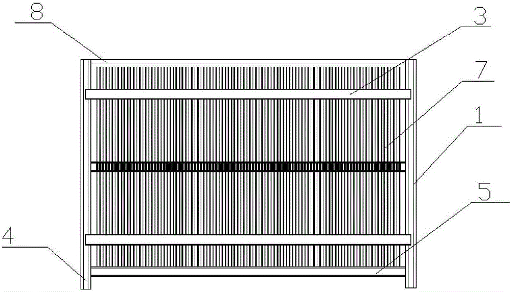
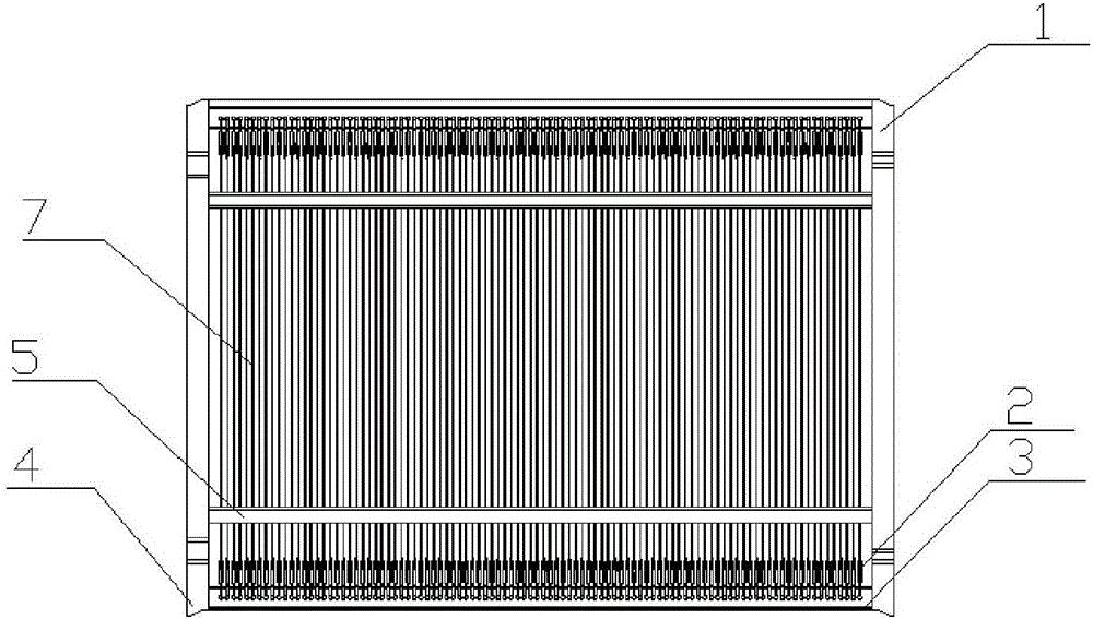
[0033] Such as Figure 4 As shown, the spring clip 2 is composed of a connecting end and a pair of elastic pieces extending outward from the connecting end, the two elastic pieces are arranged opposite to each other, and the elastic pieces are close to each other on the side away from the connecting end to form a clamping portion 10; The elastic pieces approach each other along a certain arc in the clamping portion and the part with the smallest distance is not at the end of the elastic piece. The end of the clamping portion has a curved arc concave toward the middle of the two elastic pieces, and the silicon chip 7 is clamped in the clamping portion.

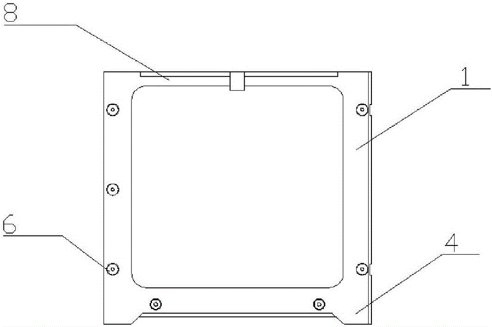
[0034] A clamping portion 9 is provided on the connecting end of the elastic piece close to the spring clip 2 , and the clamping portion 9 is clamped to the base 3 .

[0035] Such as Figure...


PUM

PropertyMeasurementUnit
thicknessaaaaaaaaaa

Abstract

The invention discloses a spring clamping piece which consists of a connection end and a pair of elastic slices extending from the connection end to the outer side, wherein the two elastic slices are opposite to each other, and the ends, far away from the connection end, of the elastic slices get close to each other to form a clamping part; and the elastic slices get close to each other at the clamping part along a certain radian, and the positions, the distance between which is smallest, are not located at the end parts of the elastic slices. The invention discloses a carrier device for clamping a silicon slice with the spring clamping piece. The carrier device consists of side plates, a base and the spring clamping piece. Two ends of the base are fixed to the side plates, and the spring clamping piece is connected into the base in a clamping manner. The device disclosed by the invention is arranged in atomic layer deposition equipment, so that a high-quality thin film plated by an atomic layer deposition film plating technology can be obtained, and the problem of circle-plating caused by the atomic layer deposition film plating technology can be solved.

Description

technical field [0001] The invention relates to an elastic clip and a carrier device using the elastic clip to clamp a silicon chip, which realizes that in the atomic layer deposition equipment, two silicon chips can be closely overlapped and placed, avoiding the problems caused by the atomic layer deposition coating technology. around the plating problem. Background technique [0002] In order to improve the efficiency of solar cells, a dielectric passivation layer is usually added on the backside of the cell to form a Passivated Emitter Rear Contact Solar Cell (PERC), which reduces the recombination of electrons and holes and improves the conversion efficiency of the cell. [0003] At present, in order to form a photovoltaic cell (or solar cell) with a passivation emitter back contact in this field, Al2O3 is usually used as a passivation layer to be plated on the photovoltaic cell, and there are two main coating methods for the photovoltaic cell, one One is plasma-enhance...

Claims


Application Information

Patent Timeline
Patent Type & Authority Applications(China)
IPC IPC(8): C23C16/44C23C16/458H01L21/687H01L31/18
CPCC23C16/44C23C16/4581H01L21/687H01L31/18Y02P70/50
Inventor 胡彬过宇晨左敏
Owner JIANGSU MICROVIA NANO EQUIP TECH CO LTD
Why Eureka
Try Eureka