Preparation method of passivation contact structure

A technology of contact structure and diffusion method, applied in the direction of final product manufacturing, sustainable manufacturing/processing, photovoltaic power generation, etc., can solve problems such as appearance and electrical performance degradation, improve cell efficiency, reduce parasitic absorption, and simple process steps Effect

Inactive Publication Date: 2020-04-24
江苏杰太光电技术有限公司
View PDF4 Cites 5 Cited by
  • Summary
  • Abstract
  • Description
  • Claims
  • Application Information

AI Technical Summary

Problems solved by technology

This method can well prepare single-sided polysilicon thin films without wrapping plating on the other side, and can adjust a reasonable doping ratio according to actual process requirements, which can solve the problems in the industrialization process of solar cells with passivated contact structures. Appearance and electrical performance degradation issues

Method used


Image

  • Preparation method of passivation contact structure
  • Preparation method of passivation contact structure
  • Preparation method of passivation contact structure

Examples


Embodiment 1

[0046] A method for preparing a passivation contact structure by physical vapor deposition (PVD) provided in the present embodiment 1 adopts the multi-source magnetron sputtering method in the physical vapor deposition to prepare a passivation contact structure, which specifically includes the following steps:

[0047] Steps (1), (2), (3), (4) and steps (1), (2), (3),

[0048] (4) the same;

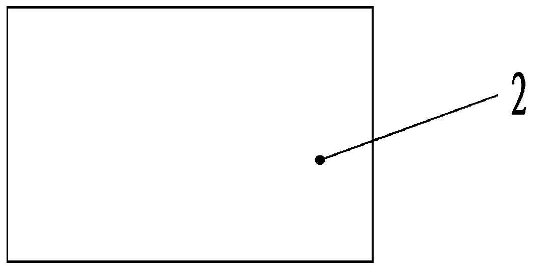
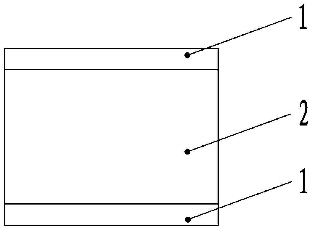
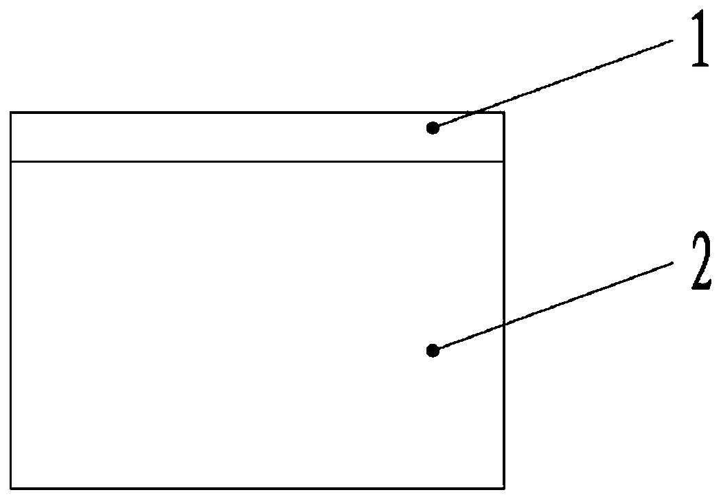
[0049] (5) The multi-source magnetron sputtering method firstly fixes the N-type silicon substrate 2 in the reaction chamber of the magnetron sputtering coater, then fixes the doped target material phosphorus or boron, and finally fixes it after the treatment in step (4). The N-type silicon substrate 2 is placed so that the side with the oxide layer faces outward and is opposite to the target, and the distance between each target and the N-type silicon substrate 2 is controlled to be 15-300mm; finally, the entire vacuum chamber is evacuated, Make its vacuum degree not higher than 1.5×10 ...

Embodiment 2

[0053] The second embodiment is to obtain a phosphorus-doped amorphous silicon layer by vacuum evaporation, and then combine with rapid thermal annealing to obtain an n-type doped passivation contact structure, which specifically includes the following steps:

[0054] Steps (1), (2), (3), (4) are the same as steps (1), (2), (3), (4) in Comparative Example 1;

[0055] (5) Multi-source co-evaporation method First, place the base evaporation source monocrystalline silicon or polycrystalline silicon powder with a purity of 99.9999% in the molybdenum boat, and then place the doped evaporation source phosphorus powder or boron powder with a purity of 99.9999% in the appropriate amount. In another molybdenum boat, each evaporation source is sequentially fixed in the vacuum coating machine, and after the end, the substrate silicon wafer processed in step 4 is fixed, so that the side with the oxide layer faces outward and is opposite to the evaporation source; finally, the substrate is ...


PUM

PropertyMeasurementUnit
thicknessaaaaaaaaaa
electrical resistivityaaaaaaaaaa
thicknessaaaaaaaaaa

Abstract

The invention relates to a preparation method of a passivation contact structure. The preparation method comprises the steps of (1) cleaning a silicon wafer substrate; (2) preparing a single-sided n<+> or p<+> doped layer on the surface of the cleaned silicon wafer; (3) depositing a tunneling oxide layer on a non-doped surface; (4) depositing a layer of doped polycrystalline silicon film on the surface of the tunneling oxide layer by adopting a PVD method. Therefore, the passivation contact structure is prepared. The method disclosed by the invention has the main advantages that the doped polycrystalline silicon film is prepared by adopting the PVD method, so that the components of the film can be well controlled; the optimal doping ratio can be debugged according to actual process requirements; the polycrystalline silicon film prepared through single-side film forming is high in deposition rate and good in compactness; and the problems that in the industrialization process of an existing solar cell in an N-type passivation contact structure, the front face appearance is poor, and the electrical property is reduced can be well solved.

Description

technical field [0001] The invention relates to the technical field of solar cell preparation, in particular to a preparation method of a passivation contact structure. Background technique [0002] In crystalline silicon solar cells, since there is no passivation layer in the metal-semiconductor contact area, the exposed dangling bonds on the semiconductor surface are easier to capture electrons, which increases the recombination of the metal contact area. In order to reduce such recombination, most of the mainstream crystalline silicon cells on the market use the emitter design with shallow junction and high square resistance, but there is still a large recombination loss. For P-type silicon cells, the dark saturation of the front surface metal contact area The current density is 800~1000fA / cm 2 , for N-type silicon cells, the dark saturation current density in the front surface contact area is 1000-2000 fA / cm 2 . At the same time, the contact between the metal and the ...

Claims


Application Information

Patent Timeline
Patent Type & Authority Applications(China)
IPC IPC(8): H01L31/18
CPCH01L31/1804Y02E10/547Y02P70/50
Inventor 陈嘉赵影文马丽敏林建伟刘志锋
Owner 江苏杰太光电技术有限公司
Why Eureka
Try Eureka