Manufacturing method of multi-layer flexible circuit board, multi-layer flexible circuit board and mobile terminal

A technology for flexible circuit boards and manufacturing methods, which is applied in multilayer circuit manufacturing, printed circuit manufacturing, and printed circuits. The effect of precision device welding

Inactive Publication Date: 2016-07-20
GUANGDONG OPPO MOBILE TELECOMM CORP LTD
View PDF3 Cites 5 Cited by
  • Summary
  • Abstract
  • Description
  • Claims
  • Application Information

AI Technical Summary

Problems solved by technology

The inventor found the following defects when making the above-mentioned multi-layer flexible circuit board: the electroplating via hole may cause via hole breakage and signal cracking due to too thin copper plating or uneven copper thickness in the hole

Method used


Image

  • Manufacturing method of multi-layer flexible circuit board, multi-layer flexible circuit board and mobile terminal
  • Manufacturing method of multi-layer flexible circuit board, multi-layer flexible circuit board and mobile terminal
  • Manufacturing method of multi-layer flexible circuit board, multi-layer flexible circuit board and mobile terminal

Examples


Embodiment Construction

[0040] Below will combine in the embodiment of the present invention Attached picture , clearly and completely describe the technical solutions in the embodiments of the present invention, obviously, the described embodiments are only some of the embodiments of the present invention, not all of them. Based on the embodiments of the present invention, all other embodiments obtained by persons of ordinary skill in the art without making creative efforts belong to the protection scope of the present invention.

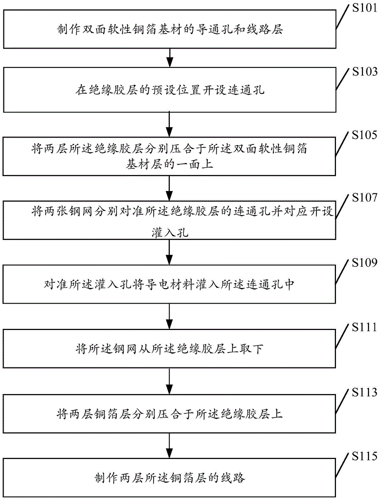
[0041] See figure 1 , is a flow diagram of a method for manufacturing a multi-layer flexible circuit board provided by an embodiment of the present invention picture . Such as figure 1 As shown, the method in this embodiment of the present invention may include the following steps S101-S113.

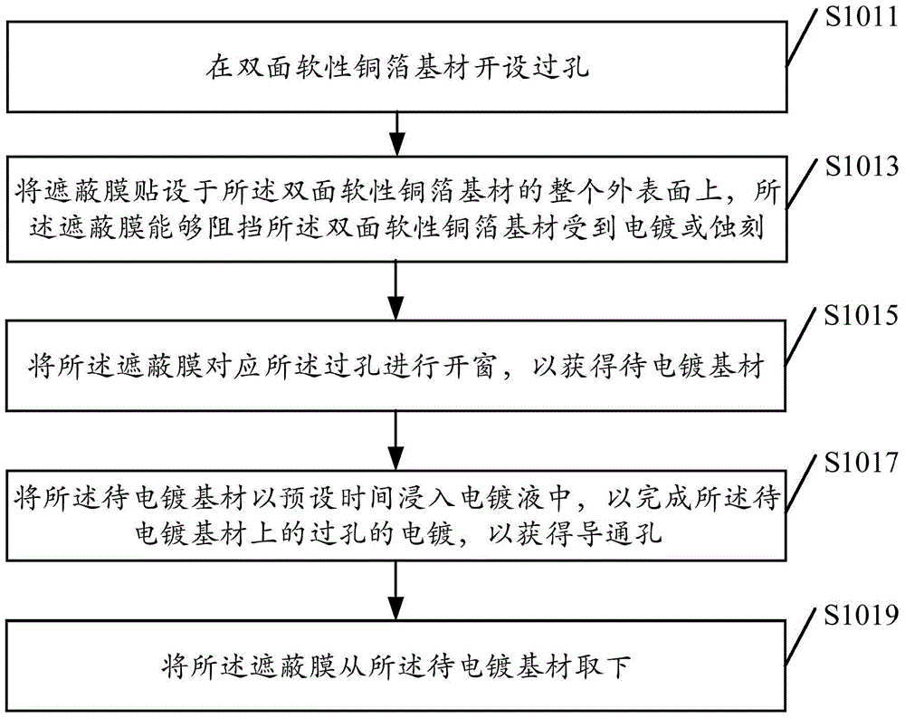
[0042] S101: Making via holes and circuit layers of double-sided flexible copper foil substrates;

[0043] Specifically, the double-sided flexible copper foil substrate i...


PUM


Abstract

The invention discloses a manufacturing method of a multi-layer flexible circuit board. The method comprises the following steps: manufacturing via holes and circuit layers on a double-sided soft copper foil substrate; forming interconnecting holes in preset positions of insulating adhesive layers; laminating each insulating adhesive layer on one surface of the double-sided soft copper foil substrate; making two steel meshes aligned with the via holes of the insulating adhesive layers respectively and correspondingly forming injection holes; injecting a conductive material into the interconnecting holes through aligning with the injection holes; taking down the steel meshes from the insulating adhesive layers; laminating two copper foil layers on the insulating adhesive layers respectively; and manufacturing a circuit with the two copper foil layers. According to the manufacturing method of the multi-layer flexible circuit board, the electric connection relationship between the copper foil layers of the multi-layer flexible circuit board is achieved by forming the interconnecting holes in the insulating adhesive layers and injecting the conductive material into the interconnecting holes; and electroplating again after holes are formed in the copper foil layers is avoided, so that uniform thickness of the multi-layer flexible circuit board is ensured; and welding of a precision device is facilitated. The invention further provides the multi-layer flexible circuit board and the mobile terminal.

Description

technical field [0001] The invention relates to the field of circuit boards, in particular to a method for manufacturing a multilayer flexible circuit board, a flexible circuit board and a mobile terminal. Background technique [0002] The manufacturing method of the existing multi-layer flexible circuit board (taking the three-layer circuit board as an example) is generally: making the FCCL inner layer board, drilling holes and making the circuit layer on the inner layer board; then symmetrically pressing on both sides of the inner layer board Insulating adhesive layer; then press the copper foil layer on the insulating adhesive layer; then drill a hole in the copper foil layer, the opening of the hole reaches the insulating adhesive layer, and finally electroplate the hole to conduct each layer of copper foil layer . The inventor found the following defects when making the above-mentioned multi-layer flexible circuit board: the electroplating via hole may cause via hole b...

Claims


Application Information

Patent Timeline
Patent Type & Authority Applications(China)
IPC IPC(8): H05K3/42H05K3/46
CPCH05K3/4623H05K3/425H05K3/429H05K2201/09563
Inventor 黄占肯
Owner GUANGDONG OPPO MOBILE TELECOMM CORP LTD
Why Eureka
Try Eureka