
Silicon carbide single crystal manufacturing device

A silicon carbide single crystal and manufacturing device technology, which is applied in the direction of single crystal growth, single crystal growth, semiconductor/solid-state device manufacturing, etc., can solve the problems of slowing down the growth rate, difficult to control the temperature of the crystal growth surface accurately, and prone to damage

Inactive Publication Date: 2016-11-16
TAIZHOU BEYOND TECH
View PDF7 Cites 14 Cited by
  • Summary
  • Abstract
  • Description
  • Claims
  • Application Information

AI Technical Summary

Problems solved by technology

The heater heats the large environment in the furnace body, so it is difficult to precisely control the temperature of the crystal growth surface, and the current method is to directly set the temperature of the crystal growth surface at about 2250°C, but the carbonization directly grown at this temperature Silicon single crystals are prone to damage during subsequent mechanical processing. In order to improve the quality of silicon carbide single crystals, the growth rate can only be reduced and the growth aperture can be reduced. In order to ensure the quality of silicon carbide crystals, the growth rate and the growth aperture can also be reduced Leading to the high cost of silicon carbide single crystal

Method used


Image

  • Silicon carbide single crystal manufacturing device
  • Silicon carbide single crystal manufacturing device
  • Silicon carbide single crystal manufacturing device

Examples


Embodiment 1

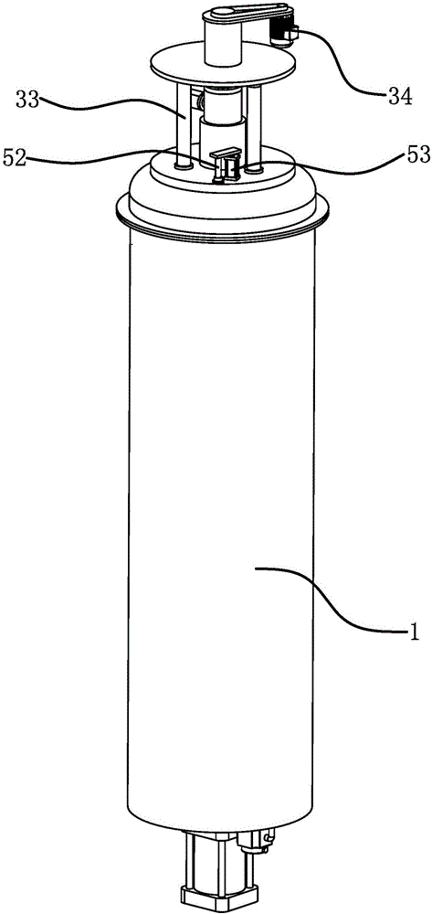
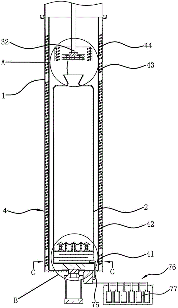
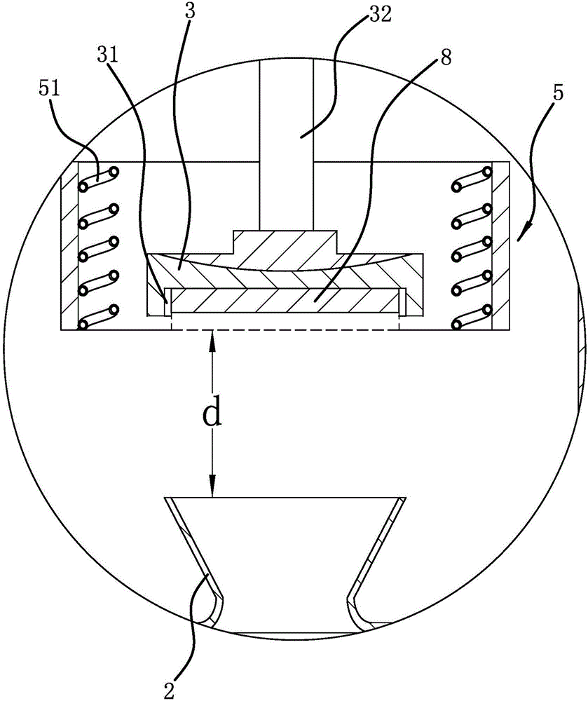
[0039] Such as figure 1 , figure 2 , image 3 As shown, a silicon carbide single crystal manufacturing device includes a furnace body 1 and a crucible 2 arranged in the furnace body 1, silicon carbide powder is placed in the crucible 2, and a seed crystal holder 3 is arranged on the upper part of the crucible 2, and the seed crystal is kept A seed crystal 8 is installed on the frame 3, and the seed crystal holder 3 can rotate and lift up and down, that is, the upper end of the furnace body 1 is rotatably connected with a lifting shaft 32. 3 is installed on the lower end of the lifting shaft 32, and the upper end of the lifting shaft 32 is respectively connected with a motor 34 that can drive the lifting shaft 32 to rotate and a cylinder one 33 that can drive the lifting shaft 32 up and down. In the furnace body 1, a furnace body heater 4 is also provided, and the furnace body heater 4 can heat the furnace body 1 to form an ambient temperature gradient in the furnace body 1,...

Embodiment 2

[0052] The structure of the silicon carbide single crystal manufacturing device is basically the same as that of Embodiment 1, the difference is that Figure 8 As shown, the upper end of the seed crystal holder 3 faces downward arc-shaped concave, then cooperates with the setting of the parameter controller, and heats the outside of the grown silicon carbide single crystal through the heating cooler 5, so that the temperature gradient of the crystallization surface is maintained. Increase or decrease within the range of 0.5°C / mm to 20°C / mm.

Embodiment 3

[0054] The structure of the silicon carbide single crystal manufacturing device is basically the same as that of Embodiment 1, the difference is that Figure 9 As shown, the upper end surface of the seed crystal holder 3 has a flat-bottomed concave cavity.


PUM


Abstract

The invention provides a silicon carbide single crystal manufacturing device, belonging to the technical field of semiconductor mechanical equipment and solving the problem that the post-mechanical processing loss of a single crystal grown by the existing silicon carbide single crystal manufacturing device is great. The silicon carbide single crystal manufacturing device comprises a furnace body and a crucible arranged in the furnace body, wherein a seed crystal retainer capable of mounting seed crystals is arranged at the upper part of the crucible; the seed crystal retainer can rotate and move up and down; a furnace body heater for heating the furnace body to enable the furnace body to form an environment temperature gradient is also arranged in the furnace body; and a heating cooler capable of acting on a silicon carbide single crystal is arranged outside the seed crystal retainer. On the premise of ensuring high quality of the silicon carbide single crystal, the silicon carbide single crystal manufacturing device grows the silicon carbide single crystal at a high speed, large-caliber growth of the silicon carbide single crystal is realized, and the post-mechanical processing loss is reduced.

Description

technical field [0001] The invention belongs to the technical field of semiconductor machinery and equipment, and relates to a silicon carbide single crystal manufacturing device. Background technique [0002] The sublimation method is currently the standard method for manufacturing silicon carbide crystals. Generally, intermediate frequency induction heating is used, that is, the silicon carbide in the crucible is heated and sublimated, and a seed crystal is placed above the crucible, so the gaseous silicon carbide rises and touches the seed crystal. After condensing and forming a silicon carbide single crystal. The heater heats the large environment in the furnace body, so it is difficult to precisely control the temperature of the crystal growth surface, and the current method is to directly set the temperature of the crystal growth surface at about 2250°C, but the carbonization directly grown at this temperature Silicon single crystals are prone to damage during subsequ...

Claims


Application Information

Patent Timeline
Patent Type & Authority Applications(China)
IPC IPC(8): C30B23/00C30B29/36
CPCC30B23/00C30B29/36C30B23/002C30B23/005C30B23/063C30B23/066H01L21/02529H01L21/02631
Inventor 星野政宏张乐年
Owner TAIZHOU BEYOND TECH
Learn More