
Pixel array and pixel structure

A pixel array and pixel structure technology, which is applied in the field of pixel array and pixel structure, can solve the problems of limiting pixel aperture ratio, light leakage, dark state light leakage, etc.

Inactive Publication Date: 2016-11-16
AU OPTRONICS CORP
View PDF6 Cites 15 Cited by
  • Summary
  • Abstract
  • Description
  • Claims
  • Application Information

AI Technical Summary

Problems solved by technology

However, in the traditional liquid crystal display panel, in order to avoid excessive coupling capacitance between the pixel electrode and the data line, there is a gap between the pixel electrode and the data line, so in the dark state, the pixel electrode cannot control the liquid crystal corresponding to the gap. Molecules, light is easy to leak out from the gap, resulting in light leakage in the dark state
Although the gap can be masked by the black matrix, this design will limit the aperture ratio of the pixel

Method used


Image

  • Pixel array and pixel structure
  • Pixel array and pixel structure
  • Pixel array and pixel structure

Examples


Embodiment Construction

[0057] In order to enable those who are familiar with the technical field of the present invention to further understand the present invention, the preferred embodiments of the present invention are enumerated below, together with the accompanying drawings, to describe in detail the composition of the present invention and the desired effects .

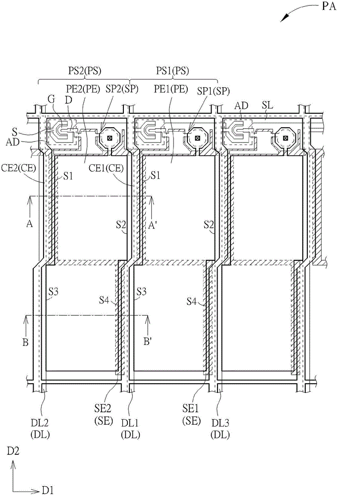
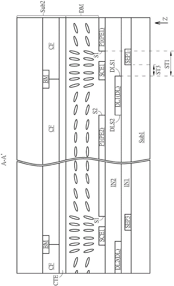
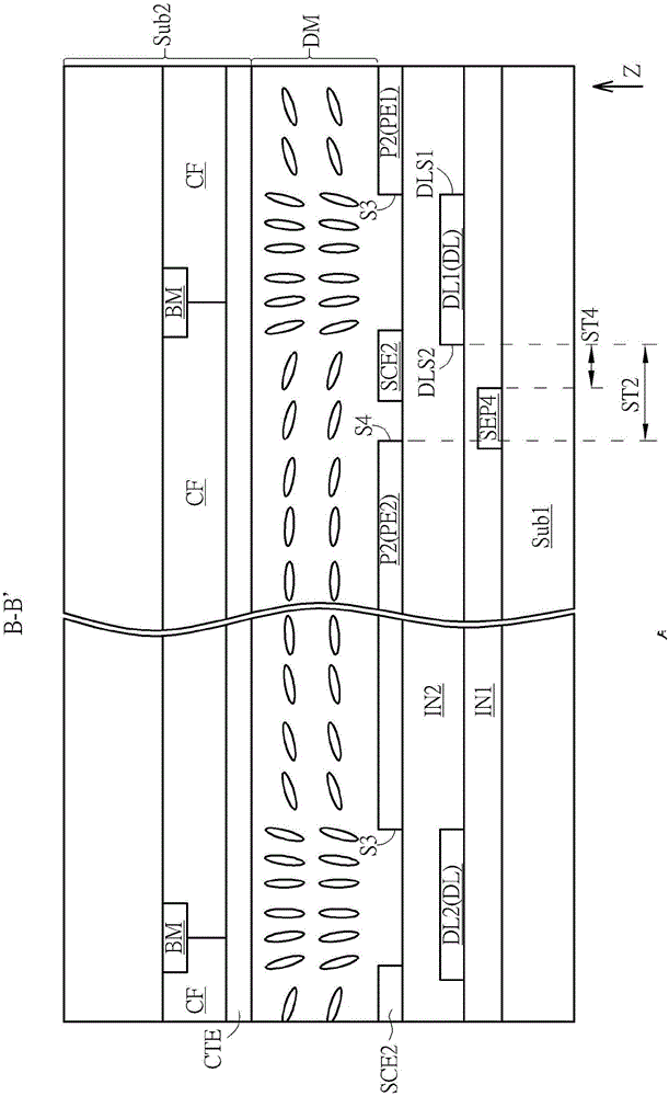
[0058] Please refer to Figure 1 to Figure 3 , figure 1 A schematic top view of the pixel array according to the first embodiment of the present invention is shown, figure 2 drawn along the figure 1 A schematic cross-sectional view of section line A-A', image 3 drawn along thefigure 1 Schematic cross-sectional view of section line B-B'. Such as Figure 1 to Figure 3 As shown, the pixel array PA provided in this embodiment may include a plurality of pixel structures PS arranged in an array. To clearly show the pixel array PA, figure 1 Only three pixel structures PS arranged in the same row (that is, arranged in the first direc...


PUM


Abstract

The invention provides a pixel array and a pixel structure. The pixel array comprises a substrate, sub-pixels, data lines, and common electrodes. The sub-pixels are disposed on the substrate, and comprise pixel electrodes and shielding electrodes. The data lines are disposed between the sub-pixels, and slits are arranged between the pixel electrodes and the data lines. The common electrodes are arranged along the data line, and comprise first common electrodes and second common electrodes, which are electrically connected together. The common electrodes and the shielding electrodes, and the slits are in a superposed arrangement.

Description

technical field [0001] The present invention relates to a pixel array and a pixel structure, in particular to a pixel array and a pixel structure of a high-contrast liquid crystal display panel. Background technique [0002] Liquid crystal display panels have been widely used in various electronic products, such as smart phones, notebook computers, and tablet PCs, due to their advantages of being light, thin, small, and energy-saving. In order to provide a wide viewing angle display effect, a polymer-stabilized alignment (Polymer-Stabilized Alignment, PSA) liquid crystal display panel has been widely used to make high-contrast and wide-viewing-view displays, such as televisions (TVs), monitors (Monitors) ), notebook computer (notebook computer) and Kanban (Public Information Display) for public information transmission. The method of making polymer-stabilized alignment liquid crystal display panels is to add a small amount of photocurable alignment monomer to the liquid cry...

Claims


Application Information

Patent Timeline
Patent Type & Authority Applications(China)
IPC IPC(8): G02F1/1343
CPCG02F1/134309
Inventor 刘维勲李珉泽陈奎百
Owner AU OPTRONICS CORP
Learn More