
Methods and compositions for forming solder bumps on a substrate with radiation curable or thermal curable solder flux

A technology of radiation curing and flux, applied in the direction of welding/cutting media/materials, assembling printed circuits with electrical components, welding equipment, etc.

Inactive Publication Date: 2016-11-16
INDIUM CORP
View PDF5 Cites 7 Cited by
  • Summary
  • Abstract
  • Description
  • Claims
  • Application Information

AI Technical Summary

Problems solved by technology

However, this material is not used as a functional material combined with flux to form a multifunctional material

Method used


Image

  • Methods and compositions for forming solder bumps on a substrate with radiation curable or thermal curable solder flux
  • Methods and compositions for forming solder bumps on a substrate with radiation curable or thermal curable solder flux
  • Methods and compositions for forming solder bumps on a substrate with radiation curable or thermal curable solder flux

Examples


Embodiment Construction

[0017] The methods and compositions disclosed herein relate to radiation curable (eg, by UV, visible light, or electron beam UV), thermally curable, or dual-curable flux compositions, and methods of processing such compositions. The flux composition can be used to form solder joints or solder bumps, and it can be exposed to heat, exposed to radiation (e.g., UV light, visible light, or electron beam), or exposed to two Those who solidify.

[0018] The cured flux can be used to strengthen solder bumps or joints, or in the case of semiconductor components to protect substrates such as printed circuit boards, electronics or silicon (or other semiconductor materials). Thus, by providing flux in combination with radiation curable, heat curable, or dual curable materials to form solder bumps and simultaneously form around the solder bumps as a support coating in semiconductor components and electronic devices The protective film of the embodiment can reduce processing steps. Thus, ...


PUM


Abstract

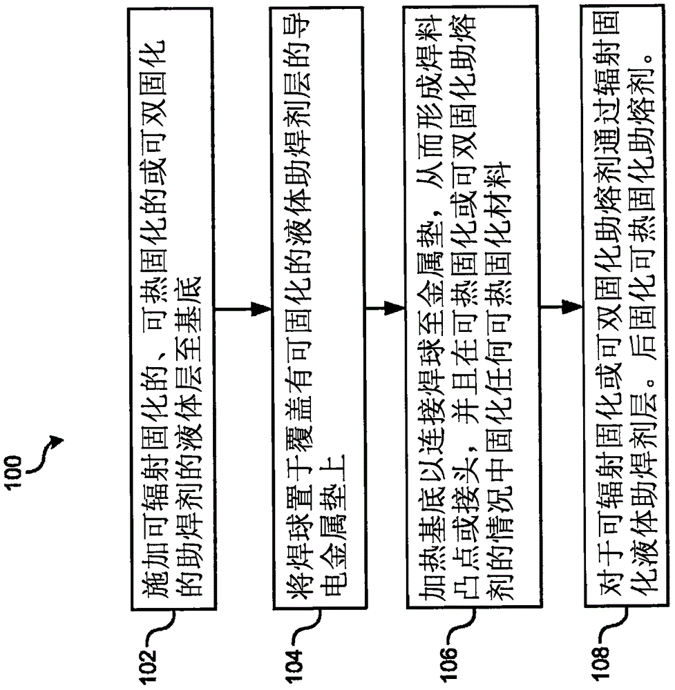
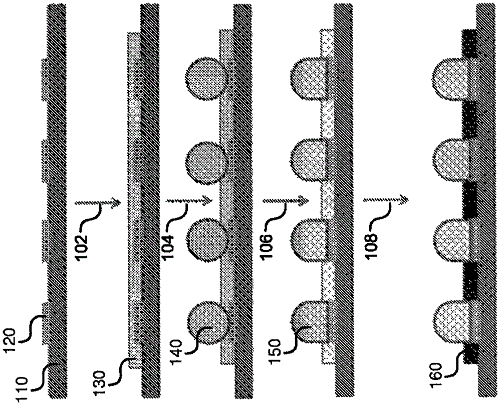
Methods of forming solder bumps or joints using a radiation curable, thermal curable solder flux, or dual curable solder fluXare disclosed. The method includes applying a liquid solder fluX130 that is radiation curable or thermal curable to a substrate 110 such that the solder fluXcovers contact padsl20 on the substrate; placing solder balls 140 on the contacts pads covered with the radiation curable or thermal curable solder flux; heating the substrate to join the solder balls to the contact pads, thereby forming solder bumps or solder joints 150; and curing the liquid solder fluXby applying radiation or heat to the substrate, thereby forming a solid film 160. The solder fluXincludes radiation curable, thermally curable, or dual curable materials that aid formation of solder bumps or joints before the solder fluXis cured; and are curable to form a solid material by the application of radiation or heat.

Description

technical field [0001] The present invention generally relates to flux compositions and methods of using the same, and more particularly, some embodiments relate to forming solder bumps using radiation-curable, heat-curable, or dual-curable fluxes. ) or joint method. Background technique [0002] An integrated circuit (IC) includes various elements (eg, transistors, diodes, resistors, capacitors, etc.) connected together by conductive materials to form a functional circuit. In many commercial implementations, the IC includes copper pads on which solder bumps are formed so that the IC can be later mounted on a printed circuit board (PCB). [0003] Reflow soldering is a well-known, conventional process in which solder paste (eg, a mixture of solder powder and flux) temporarily connects electronic devices, such as ICs, to their corresponding contact pads on a PCB. The entire assembly is then heated in a controlled manner to melt the solder that connects the electronics. Afte...

Claims


Application Information

Patent Timeline
Patent Type & Authority Applications(China)
IPC IPC(8): H05K3/34B23K1/20C08K5/09H01L23/00
CPCB23K1/0016B23K1/008B23K1/203B23K3/0623B23K35/3612B23K35/3613B23K35/362B23K2101/42C08K5/09H01L24/11H01L24/13H01L2224/03828H01L2224/10126H01L2224/11011H01L2224/11334H01L2224/11849H01L2224/131H05K3/3436H05K3/3452H05K3/3478H05K3/3489H05K2201/099H05K2201/10674H05K2203/041H05K2203/043H01L24/81H01L2924/014
Inventor M·胡N-C·李
Owner INDIUM CORP
Learn More