LED chip structure and manufacturing method thereof

A technology of LED chips and manufacturing methods, which is applied in the direction of electrical components, circuits, semiconductor devices, etc., can solve problems such as unsatisfactory luminous efficiency, reduce the probability of total reflection, reduce the probability of total reflection problems, and increase transmittance Effect

Inactive Publication Date: 2016-11-23
ENRAYTEK OPTOELECTRONICS
View PDF12 Cites 2 Cited by
  • Summary
  • Abstract
  • Description
  • Claims
  • Application Information

AI Technical Summary

Problems solved by technology

[0004] However, even if the existing LED chip structure is changed to the above-mentioned flip-chip structure, its luminous efficiency is still not ideal.

Method used


Image

  • LED chip structure and manufacturing method thereof
  • LED chip structure and manufacturing method thereof
  • LED chip structure and manufacturing method thereof

Examples


Embodiment Construction

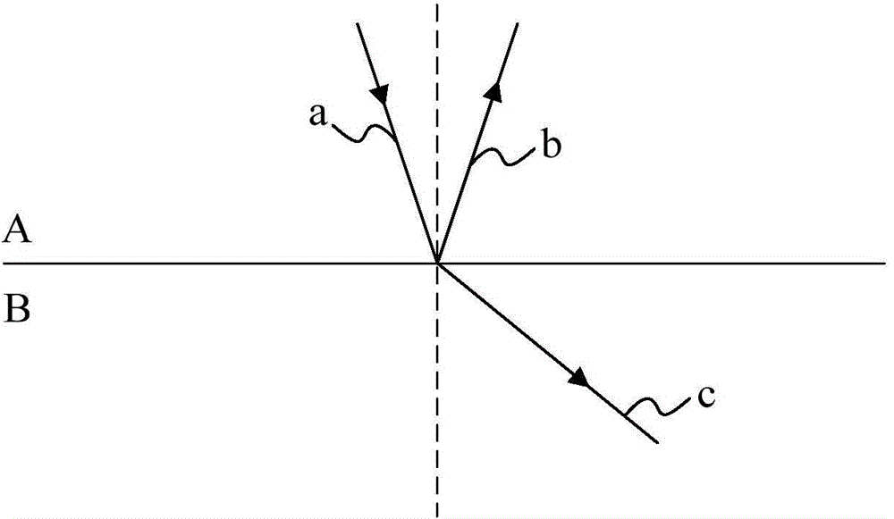
[0048] When the flip-chip LED chip structure in the prior art is in operation, the light emitted by it will be transmitted through the substrate.

[0049] However, the refractive index of the substrate used in the LED chip structure in the prior art is quite different from that of air, please refer to figure 1 , wherein A medium represents the substrate of the LED chip structure in the prior art, medium B represents the air, and the light a generated by the LED chip structure is transmitted from the substrate to the air, but the light is transmitted from the solid substrate as an optically dense When the medium enters an optically sparse medium with a refractive index close to 1, refraction will occur (please refer to light c). When the refractive index of the substrate is greatly different from that of the air, it is easy to cause total reflection of the light that should have entered the air ( Please refer to ray b) re-entering the substrate.

[0050] This will affect the l...


PUM


Abstract

The invention provides an LED chip structure and a manufacturing method thereof. The manufacturing method comprises that a substrate including a front side and a back side is provided; an N type semiconductor layer, an active layer and a P type semiconductor layer are formed successively; an N electrode and a P electrode are formed; and a buffer layer whose reflective index is lower than that of the substrate is formed. The LED structure comprises the substrate, an N type semiconductor layer, an active layer, a P type semiconductor layer, the N electrode, the P electrode and the buffer layer, wherein the N electrode and the P electrode are electrically connected with the N type semiconductor layer and the P type semiconductor layer respectively, and the buffer layer is formed in the back side of the substrate. The LED chip structure and the manufacturing method thereof have the advantages that the buffer layer whose refractive index is lower than that of the substrate is added, the possibility that light transmitted from the substrate generates total reflection is reduced, the possibility that light generates total reflection at the surface of the substrate is reduced, the light transmissivity is improved, and further the brightness of the LED chip structure is improved.

Description

technical field [0001] The invention relates to the technical field of LED manufacturing, in particular to an LED chip structure and a manufacturing method thereof. Background technique [0002] A light emitting diode (Light Emitting Diode, LED) is a semiconductor solid-state light-emitting device, which is made using the principle of semiconductor PN junction electroluminescence. LED devices have good photoelectric properties such as low turn-on voltage, small size, fast response, good stability, long life, and no pollution. Therefore, they are widely used in outdoor and indoor lighting, backlighting, display, traffic indication and other fields. [0003] Generally speaking, the LED chip structure is divided into three types: horizontal structure (front chip), vertical structure (vertical structure chip) and flip chip structure (flip chip); among them, the P and N electrodes in the flip structure LED chip are located On the same side of the light-emitting area, the light e...

Claims


Application Information

Patent Timeline
Patent Type & Authority Applications(China)
IPC IPC(8): H01L33/00H01L33/12
Inventor 朱秀山徐慧文李智勇朱广敏余婷婷张宇李起鸣
Owner ENRAYTEK OPTOELECTRONICS
Why Eureka
Try Eureka