Cutting device of semiconductor material or non-conductive material using wire electric discharge processing, and method of the same

A discharge machining and non-conductor technology, which is applied in the direction of electric processing equipment, fine working devices, accessory devices, etc., can solve the problem that the shape of the cutting is not fine and complete.

Inactive Publication Date: 2016-12-07
郭俊良
View PDF7 Cites 2 Cited by
  • Summary
  • Abstract
  • Description
  • Claims
  • Application Information

AI Technical Summary

Problems solved by technology

[0007] However, due to the traditional cutting process for poor thermoelectric conductors, it is difficult and the shape of the cutting is not fine and complete.

Method used


Image

  • Cutting device of semiconductor material or non-conductive material using wire electric discharge processing, and method of the same
  • Cutting device of semiconductor material or non-conductive material using wire electric discharge processing, and method of the same
  • Cutting device of semiconductor material or non-conductive material using wire electric discharge processing, and method of the same

Examples


Embodiment

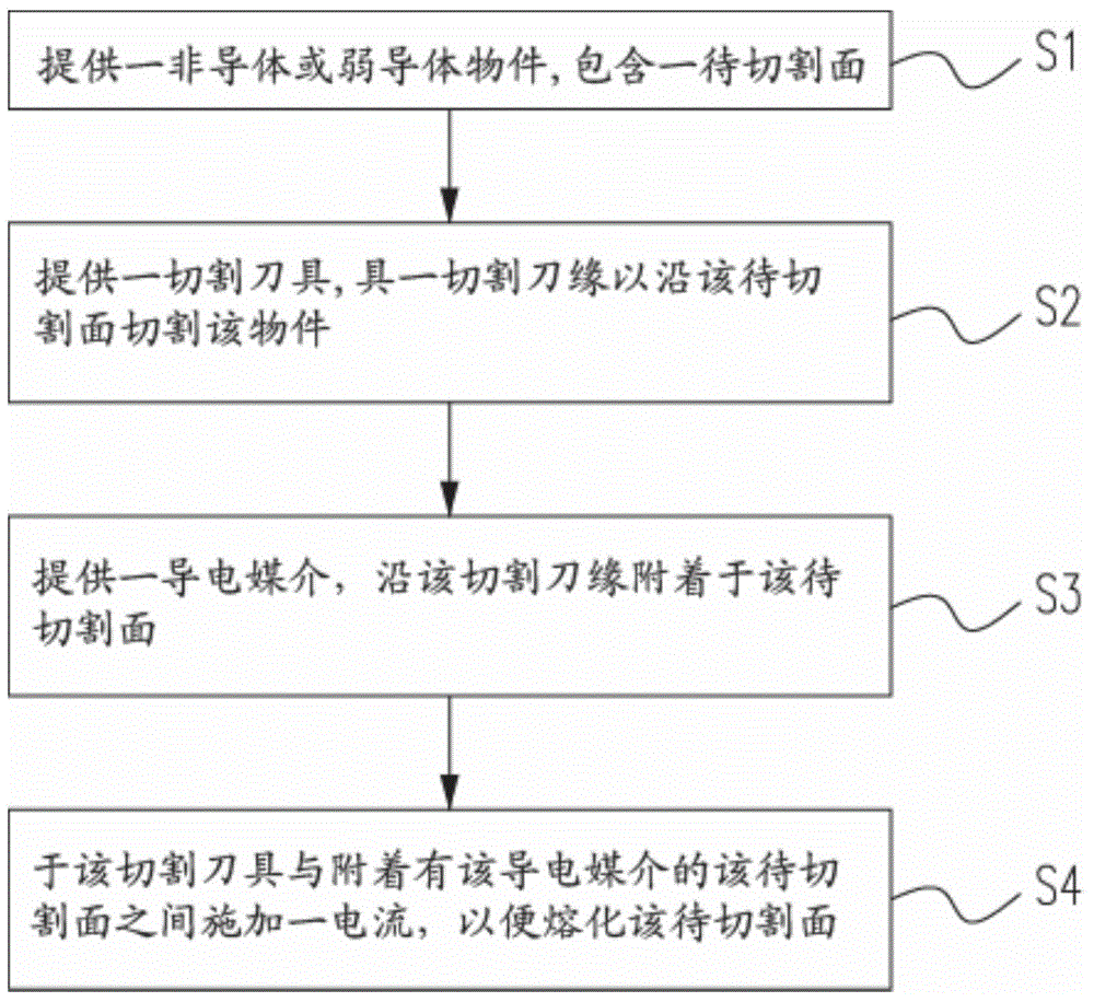
[0055] 1. A wire discharge machining method, comprising: (a) providing a non-conductor or weak conductor object, comprising a surface to be cut; (b) providing a cutting wire or cutter, with a cutting edge to be cut along the surface to be cut cutting the object; (c) providing a conductive medium attached to the surface to be cut along the cutting edge; and (d) applying an electric current between the cutting wire or cutter and the surface to be cut to which the conductive medium is attached , in order to melt the surface to be cut.

[0056] 2. The wire electric discharge machining method as described in embodiment 1, further comprising step (e): repeating steps (c)-(d).

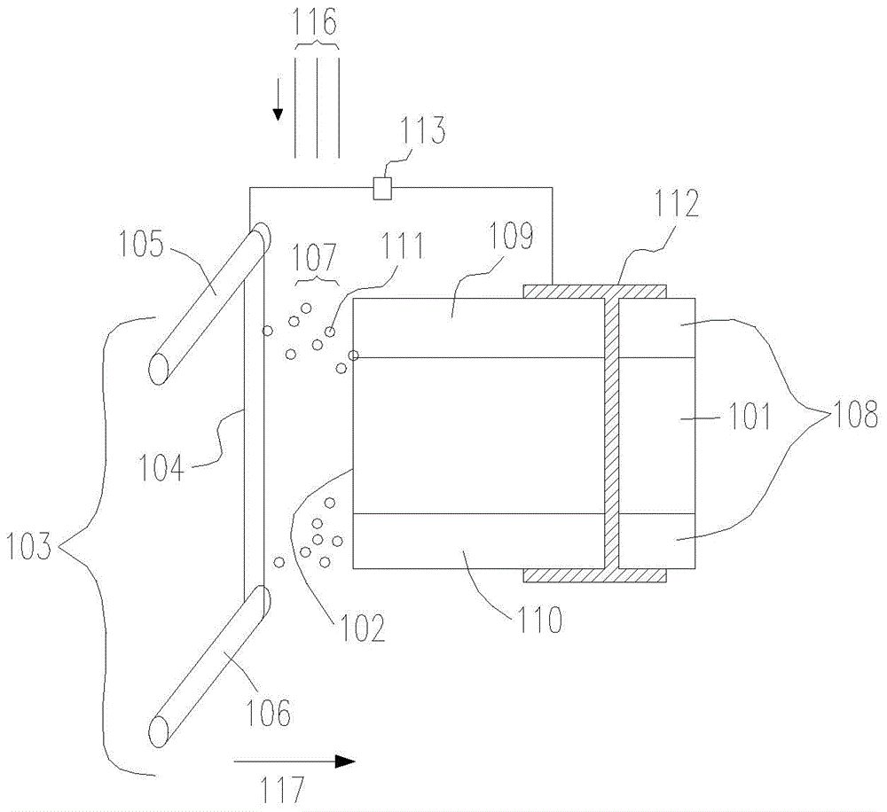
[0057] 3. The wire discharge machining method as described in embodiment 1 or 2, wherein the object has a surface adjacent to the surface to be cut, and step (c) further includes (c1) providing a conductive medium supply source, the conductive The medium supply source is a metal plate arranged on the surface...

Embodiment 8

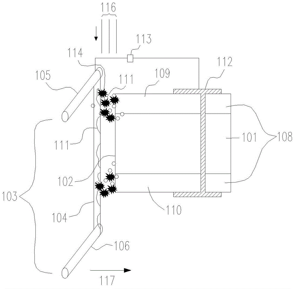
[0061] According to the wire electric discharge machining method described in any one of the embodiments 3 to 7 of the present invention, step (d) further includes: (d1) moving the cutting wire or the cutter to the edge near the conductive medium supply source and the to-be-cut moving in a first direction of the surface, and applying the current to the cutting wire or cutter in contact with the edge of the conductive medium supply and the surface to be cut; and (d2) moving the cutting wire or cutter away from the conductive medium supply The edge of the edge and the surface to be cut move in a second direction.

Embodiment 9

[0063] The wire discharge machining method according to one of the embodiments 3-8 of the present invention, wherein in the step (c), the conductive medium penetrates further into the surface to be cut.


PUM


Abstract

A wire electrical discharge machining (WEDM) method is disclosed, the WEDM method comprising steps of: (a) providing one of a non-conductive and a weakly conductive object having a to-be-cut surface; (b) providing one of a wire and a cutting tool having a cutting blade edge to cut the object along the to-be-cut surface; (c) providing a conductive medium to adhere to the to-be-cut surface via the cutting blade edge; and (d) applying an electric current between the one of the wire and the cutting tool, and the to-be-cut surface adhered to the conductive medium such that the to-be-cut surface is melted.

Description

technical field [0001] The present invention relates to a wire discharge processing device and method thereof, in particular to a wire discharge processing device and method applied to non-conductors or weak conductors, wherein a weak conductor refers to a poor thermoelectric conductor. Background technique [0002] Existing cutting technologies for non-conductors or weak conductors rely on traditional abrasive wire strip cutting. The cutting stress generated by it will cause workpiece breakage and dimensional variation, resulting in many negative effects, such as thickness restrictions and precision of cutting parts In addition, the processing efficiency and material removal rate are reduced, and when it is applied to the cutting operation of semiconductors, it also involves the burden of material selection and manufacturing costs. [0003] In addition, a layer of conductive resin is plated on the polished single crystal silicon plate, roughed in water, and finally finished...

Claims


Application Information

Patent Timeline
Patent Type & Authority Applications(China)
IPC IPC(8): B28D5/00
CPCB23H7/02B23H7/04B23H11/00
Inventor 郭俊良郑正元
Owner 郭俊良
Why Eureka
Try Eureka