Transistor small-signal equivalent circuit model containing intrinsic inductor, and parameter extraction method

An equivalent circuit model and small signal technology, which is applied in the fields of electrical digital data processing, CAD circuit design, special data processing applications, etc., can solve the problem that the high-precision simulation of transistors cannot be realized, the inductance effect is not considered, and the equivalent circuit model cannot be realized High-precision fitting and other issues

Active Publication Date: 2016-12-07
BROAD CHIP NANJING COMM TECH CO LTD +1
View PDF9 Cites 11 Cited by
  • Summary
  • Abstract
  • Description
  • Claims
  • Application Information

AI Technical Summary

Problems solved by technology

In the subsequent comparison of the test results and the simulation results, we show that the high-precision fitting between the equivalent circuit model and the test results cannot be achieved only through the parasitic inductance
[0012] The inductance effect that has been considered in the traditional transistor small-signal equivalent circuit model is only reflected in the parasitic part, but the internal current flow of the transistor will also produce inductance effect, this intrinsic inductance effect has not been considered by the traditional transistor small-signal equivalent circuit model
More importantly, the value of the intrinsic inductance component changes with the change of the bias. This characteristic will not be reflected by adjusting the parasitic inductance in the traditional transistor small-signal equivalent circuit model. Therefore, the traditional transistor small-signal equivalent circuit model High-precision simulation of transistors cannot be achieved
[0013] To sum up, the existing international small-signal equivalent circuit models of transistors do not consider the intrinsic inductance element existing in the intrinsic part, so the traditional small-signal equivalent circuit model of transistors cannot achieve high-precision fitting of the same test results

Method used


Image

  • Transistor small-signal equivalent circuit model containing intrinsic inductor, and parameter extraction method
  • Transistor small-signal equivalent circuit model containing intrinsic inductor, and parameter extraction method
  • Transistor small-signal equivalent circuit model containing intrinsic inductor, and parameter extraction method

Examples


Embodiment approach

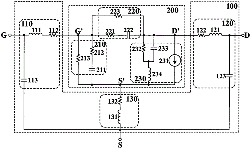
[0066] Such as figure 1 As shown, the field effect transistor small-signal equivalent circuit model includes a parasitic part (100) and an intrinsic part (200), wherein the parasitic part includes a gate parasitic unit (110), a drain parasitic unit (120), a source parasitic The unit (130), the intrinsic part includes an intrinsic unit between gate and source (210), an intrinsic unit between gate and drain (220), and an intrinsic unit between source and drain (230).

[0067] The intrinsic inductance element is included in the source-drain intrinsic unit (230).

[0068] The gate parasitic unit (110) is located between the gate external node (G) and the gate internal node (G'), and is connected to the gate external node (G) and the gate internal node (G'); The drain parasitic unit (120) is located between the drain outer node (D) and the drain inner node (D'), and is connected to the drain outer node (D) and the drain inner node (D'); The source parasitic unit (130) is located ...


PUM


Abstract

The invention discloses a transistor small-signal equivalent circuit model, which is characterized in that the intrinsic unit of the transistor small-signal equivalent circuit model comprises an intrinsic inductance element, wherein the intrinsic inductance element is positioned between the source electrode and the drain electrode of the transistor intrinsic unit; and the specific position of the intrinsic inductance element is that the intrinsic inductance element is connected with source and drain resistors in series or is connected with the parallel whole of source and drain resistors and source and drain capacitors in series so as to realize the high-accuracy simulation of the transistor under high frequency and high current. The invention further discloses a characteristic function which contains the intrinsic inductor, and a method for extracting the parameter value of the intrinsic inductance element by a measured S parameter. By use of the small-signal equivalent circuit model containing the intrinsic inductor, the fitting accuracy of stimulation and a test result can be improved.

Description

Technical field [0001] The invention relates to a device model of a transistor, in particular to a small-signal equivalent circuit model of the transistor. Background technique [0002] Transistor is one of the most important components in microelectronic devices and integrated circuit chips, and has a wide range of applications in various fields. In the design process of electronic devices and integrated circuits, transistor model is an indispensable tool. Internationally, digital models of transistors are relatively mature and can provide high-precision model simulations. However, the radio frequency model of transistors is not perfect at present, which becomes a major difficulty in the design and implementation of radio frequency circuit chips. [0003] Transistor models mainly include two types, physical models and equivalent circuit models. Among them, the design of the circuit chip is mainly based on the equivalent circuit model independent of frequency. A high-pre...

Claims


Application Information

Patent Timeline
Patent Type & Authority Applications(China)
IPC IPC(8): G06F17/50
CPCG06F30/36G06F30/367
Inventor 姜楠黄风义张有明
Owner BROAD CHIP NANJING COMM TECH CO LTD
Why Eureka
Try Eureka