Method and system for improving DC voltage utilization ratio of three-phase and four-switch fault-tolerant inverter
A DC voltage, four-switch technology is applied in the field of improving the DC voltage utilization rate of a four-switch fault-tolerant inverter, which can solve the problems of reducing the load capacity, limiting the accuracy of the algorithm, and not considering the problem of the voltage imbalance of the DC side busbar capacitors.
Active Publication Date: 2016-12-07
DALIAN UNIV OF TECH
2 Cites 5 Cited by
AI-Extracted Technical Summary
Problems solved by technology
The maximum DC voltage utilization rate of the four-switch fault-tolerant inverter is only half of that of the six-switch inverter, which greatly reduces the load capacity
This method improves the output voltage of the four-switch inverter to a certain extent, thereby increasing the output torque, but the calculation of the control angle and the holding angle is either perform...
Abstract
The invention discloses a method and system for improving the DC voltage utilization ratio of a three-phase and four-switch fault-tolerant inverter. The method comprises the steps of (S1) calculating and judging whether an unbalanced coefficient epsilon of capacitor voltage at a DC side is zero or not, if so, executing the step (S3), or else, executing the step (S2); (S2) correcting four effective voltage vectors of the four-switch fault-tolerant inverter and calculating corrected voltage vector amplitudes respectively; (S3) calculating a reference voltage vector amplitude; (S4) calculating a modulation ratio parameter M on the basis of the reference voltage vector amplitude; (S5) carrying out modulation area division on a complex plane formed by the four voltage vectors; (S6) setting overmodulation algorithms corresponding to various areas respectively and selecting corresponding vectors to synthesize corresponding compensation voltage vectors; and (S7) calculating action time of two effective voltage vectors corresponding to the compensation voltage vectors and an equivalent zero vector to finish PWM modulation. By the method and the system, the DC voltage utilization rate of the inverter is improved; meanwhile, electromagnetic torque is improved; output harmonics are reduced; and the method is simple and easy to implement in engineering.
Application Domain
Ac-dc conversion
Technology Topic
Power inverterElectromagnetic torque +10
Image
Examples
- Experimental program(1)
Example Embodiment
[0173] In order to make the objectives, technical solutions and advantages of the present invention clearer, the technical solutions of the present invention will be described clearly and completely with reference to the accompanying drawings in the embodiments of the present invention. Obviously, the described embodiments are part of the implementation of the present invention. Examples, not all examples. Based on the embodiments of the present invention, all other embodiments obtained by those of ordinary skill in the art without creative work shall fall within the protection scope of the present invention.
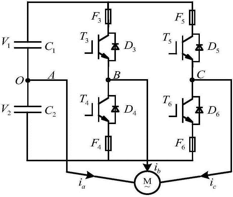
[0174] After a bridge arm (such as phase a) of the three-phase six-switch inverter fails, the main circuit topology is reconstructed to obtain the main circuit topology of the four-switch fault-tolerant inverter, such as figure 1 Shown; the present invention takes a-phase bridge arm failure as an example to illustrate the overmodulation method of a four-switch fault-tolerant inverter: according to figure 1 The combination of the different switching states of the two bridge arms can get 4 working states, among which the voltage vector U 1 ,U 2 ,U 3 ,U 4 Is 4 effective voltage vectors and divides the complex plane into 4 sectors, such as image 3 As shown, it can be seen from the figure that the amplitudes of the four voltage vectors are not equal, and the amplitude of the long vector is The magnitude of the short vector is U dc /3.
[0175] Such as figure 2 , The overmodulation method for the above-mentioned four-switch fault-tolerant inverter includes the following steps:
[0176] S1. Calculate and judge whether the DC side capacitor voltage unbalance coefficient ε of the four-switch fault-tolerant inverter is 0, if yes, execute S3, otherwise execute S2; the calculation formula of the DC side capacitor voltage unbalance coefficient ε is
[0177] ϵ = 1 2 - V 1 U d c - - - ( 1 )
[0178] In formula (1), V 1 Is the DC side capacitor C 1 Voltage across terminals, U dc Is the DC bus voltage, obviously when the DC measuring capacitor voltage is balanced, such as image 3 ,Ε=0, when ε≠0, the four voltage vector distribution diagrams are as follows Figure 4A with Figure 4B Shown.
[0179] S2, correct the four effective voltage vectors of the four-switch fault-tolerant inverter and respectively calculate the amplitude of the voltage vector corresponding to the four effective voltage vectors after the correction, and then execute S3; the corrected voltage vector is as Figure 5A with Figure 5B Shown. Among them, the four effective voltage vectors U of the four-switch fault-tolerant inverter 1 ,U 2 ,U 3 ,U 4 Make corrections to get the voltage vector U′ 1 ,U′ 2 ,U′ 3 ,U′ 4 The process is:
[0180] make
[0181] U 1 ′ = aU 1 ; U 2 ′ = bU 1 + cU 2 + dU 3 ; U 3 ′ = eU 3 ; U 4 ′ = fU 1 + gU 4 + hU 3 ; - - - ( 2 )
[0182] When V 1 ≤V 2 Time,
[0183] a = V 1 + V 2 2 V 2 ; b = 0 ; c = 1 ; d = V 2 - V 1 2 V 1 ; e = V 1 + V 2 2 V 1 ; f = 0 ; g = 1 ; h = V 2 - V 1 2 V 1 ; - - - ( 3 )
[0184] When V 1V 2 Time,
[0185] a = V 1 + V 2 2 V 2 ; b = V 1 - V 2 2 V 2 ; c = 1 ; d = 0 ; e = V 1 + V 2 2 V 1 ; f = V 1 - V 2 2 V 2 ; g = 1 ; h = 0 ; - - - ( 4 )
[0186] S3. Calculate the reference voltage vector amplitude of the four-switch fault-tolerant inverter;
[0187] S4. Based on the reference voltage vector amplitude calculated in S3, calculate the modulation ratio parameter M used to divide the modulation area of the complex plane formed by the four voltage vectors, and the calculation formula of the modulation ratio parameter M is as follows:
[0188] M = π | U r | U d c - - - ( 5 )
[0189] Where |U r | Is the reference voltage vector amplitude, U dc Is the DC bus voltage;
[0190] S5, such as Figure 5A with Figure 5B As shown, based on the calculated modulation ratio parameter M, the complex plane formed by the four voltage vectors is divided into the modulation area, that is, it is divided into linear modulation area, over modulation I area, over modulation II area and over modulation III Zone; its division principle is: linear modulation and overmodulation I zone boundary corresponding to the modulation ratio M 1 , The corresponding modulation ratio M at the boundary of overmodulation zone I and overmodulation zone II 2 , The corresponding modulation ratio M at the boundary of overmodulation area II and overmodulation area III 3 , And the corresponding modulation ratio M at the upper limit of overmodulation zone III max , That is, the range of the linear modulation area is 0 1 , The range of overmodulation I area is M 1 2 , The range of overmodulation zone II is M 2 3 , The range of overmodulation zone III is M 3 max ,
[0191] Among them, it is obtained by Fourier decomposition of the actual output voltage vector trajectory and the principle of equal output phase voltage fundamental wave amplitude:
[0192] M 1 = 0.9069 ; M 2 = 0.9517 ; M 3 = 0.9613 ; M max = 1.2216 ; - - - ( 6 ) .
[0193] S6. Set the respective overmodulation algorithms for the divided overmodulation zone I, overmodulation zone II, and overmodulation zone III, and synthesize the actual output voltage vector or of the four-switch fault-tolerant inverter based on each overmodulation algorithm Is called the compensation voltage vector; further, as a preferred solution of the present invention,
[0194] The overmodulation algorithm corresponding to the overmodulation zone I is:
[0195] First define the overmodulation coefficient corresponding to the overmodulation I area
[0196] k 1 = M - M 1 M 2 - M 1 - - - ( 7 )
[0197] Secondly, modify the reference voltage vector, such as Image 6 As shown, it includes the following:
[0198] In the first sector, when the reference voltage vector phase is [0,π/3), the weighting coefficient is (1-k 1 ) Of the inscribed circle voltage vector U rins And the weighting coefficient is k 1 The quadrilateral boundary voltage vector U rq Synthesize the compensation voltage vector. When the phase of the reference voltage vector is [π/3,π/2), the compensation voltage vector remains the same as the reference voltage vector.
[0199] which is
[0200] U r * = k 1 U r q + ( 1 - k 1 ) U r i n s , 0 ≤ θ π / 3 U r , π / 3 ≤ θ π / 2 - - - ( 8 )
[0201] among them,
[0202] U r i n s = U d c 2 3 e j θ - - - ( 9 )
[0203]
[0204] In the second sector, when the reference voltage vector phase is [π/2,2π/3), the compensation voltage vector remains the same as the reference voltage vector; when the reference voltage vector phase is [2π/3,π), the weighting coefficient Is (1-k 1 ) The inscribed circle voltage vector and the weighting coefficient is k 1 The quadrilateral boundary voltage vector synthesizes the compensation voltage vector, namely
[0205] U r * = U r , π / 2 ≤ θ 2 π / 3 k 1 U r q + ( 1 - k 1 ) U r i n s , 2 π / 3 ≤ θ π - - - ( 11 ) ;
[0206] In the third sector, when the reference voltage vector phase is [π, 4π/3), the weighting coefficient is (1-k 1 ) Of the inscribed circle voltage vector U rins And the weighting coefficient is k 1 The quadrilateral boundary voltage vector U rq Synthesize the compensation voltage vector. When the phase of the reference voltage vector is [4π/3, 3π/2), the compensation voltage vector remains the same as the reference voltage vector, that is
[0207] U r * = k 1 U r q + ( 1 - k 1 ) U r i n s , π ≤ θ 4 π / 3 U r , 4 π / 3 ≤ θ 3 π / 2 - - - ( 12 ) ;
[0208] In the fourth sector, when the reference voltage vector phase is [3π/2,5π/3), the compensation voltage vector remains the same as the reference voltage vector; when the reference voltage vector phase is [5π/3,2π), the weighting coefficient Is (1-k 1 ) The inscribed circle voltage vector and the weighting coefficient is k 1 The quadrilateral boundary voltage vector synthesizes the compensation voltage vector, namely
[0209] U r * = U r , 3 π / 2 ≤ θ 5 π / 3 k 1 U r q + ( 1 - k 1 ) U r i n s , 5 π / 3 ≤ θ 2 π - - - ( 13 ) ;
[0210] The overmodulation algorithm corresponding to the overmodulation area II is:
[0211] First define the overmodulation coefficient corresponding to the overmodulation area II
[0212] k 2 = M - M 2 M 3 - M 2 - - - ( 14 )
[0213] Secondly, modify the reference voltage vector, such as Figure 7 As shown, it includes the following:
[0214] In the first sector, when the reference voltage vector phase is [0,π/3), the compensation voltage vector is the quadrilateral boundary voltage vector U rq; When the reference voltage vector phase is [π/3,π/2), the weighting coefficient is (1-k 2 ) To M 2 U dc /π is the voltage vector U corresponding to the circle with radius rm And the weighting coefficient is k 2 The quadrilateral boundary voltage vector U rq Synthesize the compensation voltage vector, namely
[0215] U r * = U r q , 0 ≤ θ π / 3 k 2 U r q + ( 1 - k 2 ) U r m , π / 3 ≤ θ π / 2 - - - ( 15 )
[0216] among them,
[0217]
[0218] In the second sector, when the reference voltage vector phase is [π/2, 2π/3), the weighting coefficient is (1-k 2 ) To M 2 U dc /π is the radius of the circle corresponding to the voltage vector and the weighting coefficient is k 2 The quadrilateral boundary voltage vector composes the compensation voltage vector; when the phase of the reference voltage vector is [2π/3,π), the compensation voltage vector remains the quadrilateral boundary voltage vector, that is
[0219] U r * = k 2 U r q + ( 1 - k 2 ) U r m , π / 2 ≤ θ 2 π / 3 U r q , 2 π / 3 ≤ θ π - - - ( 17 )
[0220] In the third sector, when the reference voltage vector phase is [π, 4π/3), the compensation voltage vector is the quadrilateral boundary voltage vector U rq; When the reference voltage vector phase is [4π/3,3π/2), the weighting coefficient is (1-k 2 ) To M 2 U dc /π is the voltage vector U corresponding to the circle with radius rm And the weighting coefficient is k 2 The quadrilateral boundary voltage vector U rq Synthesize the compensation voltage vector, namely
[0221] U r * = U r q , π ≤ θ 4 π / 3 k 2 U r q + ( 1 - k 2 ) U r m , 4 π / 3 ≤ θ 3 π / 2 - - - ( 18 )
[0222] In the fourth sector, when the reference voltage vector phase is [3π/2,5π/3), the weighting coefficient is (1-k 2 ) To M 2 U dc /π is the radius of the circle corresponding to the voltage vector and the weighting coefficient is k 2 The quadrilateral boundary voltage vector composes the compensation voltage vector; when the phase of the reference voltage vector is [5π/3, 2π), the compensation voltage vector remains the quadrilateral boundary voltage vector, that is
[0223] U r * = k 2 U r q + ( 1 - k 2 ) U r m , 3 π / 2 ≤ θ 5 π / 3 U r q , 5 π / 3 ≤ θ 2 π - - - ( 19 ) ;
[0224] The overmodulation algorithm corresponding to the overmodulation zone III is:
[0225] First define the overmodulation coefficient corresponding to the overmodulation zone III
[0226] k 3 = M - M 3 M m a x - M 3 - - - ( 20 )
[0227] Secondly, modify the reference voltage vector, such as Figure 8 As shown, it includes the following:
[0228] In the first sector, when the reference voltage vector phase is [0,π/3), the weighting coefficient is (1-k 3 ) Quadrilateral boundary voltage vector U rq And the weighting coefficient is k 3 Effective voltage vector U rf Synthesize the compensation voltage vector; when the phase of the reference voltage vector is [π/3,π/2), the compensation voltage vector remains the quadrilateral boundary voltage vector U rq , which is
[0229] U r * = k 3 U r f + ( 1 - k 3 ) U r q , 0 ≤ θ π / 3 U r q , π / 3 ≤ θ π / 2 - - - ( twenty one )
[0230] among them,
[0231]
[0232] In the second sector, when the reference voltage vector phase is [π/2, 2π/3), the compensation voltage vector remains a quadrilateral boundary voltage vector; when the reference voltage vector phase is [2π/3, π), the weighting coefficient Is (1-k 3 ) The quadrilateral boundary voltage vector and the weighting coefficient is k 3 The short voltage vector synthesis compensation voltage vector, namely
[0233] U r * = U r q , π / 2 ≤ θ 2 π / 3 k 3 U r f + ( 1 - k 3 ) U r q , 2 π / 3 ≤ θ π - - - ( twenty three )
[0234] among them,
[0235]
[0236] In the third sector, when the reference voltage vector phase is [π, 4π/3), the weighting coefficient is (1-k 3 ) Quadrilateral boundary voltage vector U rq And the weighting coefficient is k 3 Effective voltage vector U rf Synthesize the compensation voltage vector; when the phase of the reference voltage vector is [4π/3,3π/2), the compensation voltage vector remains as the quadrilateral boundary voltage vector U rq , which is
[0237] U r * = k 3 U r f + ( 1 - k 3 ) U r q , π ≤ θ 4 π / 3 U r q , 4 π / 3 ≤ θ 3 π / 2 - - - ( 25 )
[0238] among them,
[0239]
[0240] In the fourth sector, when the reference voltage vector phase is [3π/2,5π/3), the compensation voltage vector remains as a quadrilateral boundary voltage vector; when the reference voltage vector phase is [5π/3,2π), the weighting coefficient Is (1-k 3 ) The quadrilateral boundary voltage vector and the weighting coefficient is k 3 The short voltage vector synthesis compensation voltage vector, namely
[0241] U r * = U r q , 3 π / 2 ≤ θ 5 π / 3 k 3 U r f + ( 1 - k 3 ) U r q , 5 π / 3 ≤ θ 2 π - - - ( 27 )
[0242] among them,
[0243]
[0244] S7. Calculate the action time T of the two effective voltage vectors and the equivalent zero vector corresponding to the synthesized compensation voltage vector based on the volt-second balance principle 1 , T 2 , T 0 , And then complete the corresponding PWM modulation.
[0245] Specifically, because S7 borrows the method used in the prior art, only the first sector is used as an example for description, such as Picture 9 Shown:
[0246] ∫ 0 T s U r e f * d t = ∫ 0 T 1 U 1 d t + ∫ T 1 T 1 + T 2 U 2 d t + ∫ T 1 + T 2 T s U Z d t - - - ( 29 )
[0247] Where U Z Represents a zero vector, and selects U with equal time 1 And U 3 To be equivalent, and the number is worth
[0248] T 1 = 3 T s | U r * | c o s ( θ ) U d c - - - ( 30 )
[0249] T 2 = 3 T s | U r * | s i n ( θ ) U d c - - - ( 31 )
[0250] T 0 = T s -T 1 -T 2 (32)
[0251] Where T s Is the sampling period, T 0 Is the zero vector action time; then according to T 1 , T 2 , T 0 Then complete the PWM modulation.
[0252] When the b-phase bridge arm or c-phase bridge arm of the four-switch fault-tolerant inverter fails, the modulation method of the a-phase bridge arm can be used for over-modulation control to improve the DC voltage utilization rate and load of the fault-tolerant inverter ability.
[0253] Based on the above method, such as Picture 10 The invention also provides a system for improving the DC voltage utilization rate of a four-switch fault-tolerant inverter, which is characterized in that it includes:
[0254] Unbalance coefficient calculation module, which can calculate and judge whether the DC side capacitor voltage unbalance coefficient ε of the four-switch fault-tolerant inverter is 0;
[0255] Effective voltage vector correction module, the effective voltage vector correction module can correct the four effective voltage vectors of the four-switch fault-tolerant inverter under the condition that the DC side capacitor voltage unbalance coefficient ε is not 0 and calculate the corrected four The amplitude of the voltage vector corresponding to each effective voltage vector;
[0256] A reference voltage vector amplitude calculation module, which can calculate the reference voltage vector amplitude corresponding to the four-switch fault-tolerant inverter;
[0257] Modulation ratio parameter calculation module, the modulation ratio parameter can be based on the reference voltage vector amplitude calculated by the reference voltage vector calculation module to calculate the modulation ratio parameter M used to divide the modulation area of the complex plane formed by the four voltage vectors, so The formula for calculating the modulation ratio parameter M is as follows:
[0258] M = π | U r | U d c
[0259] Where |U r | Is the reference voltage vector amplitude, U dc Is the DC bus voltage;
[0260] Modulation area division module, which can divide the modulation area of the complex plane formed by four voltage vectors based on the calculated modulation ratio parameter M, that is, divide it into linear modulation area, overmodulation I area, Overmodulation area II and overmodulation area III; the range of the linear modulation area is 0 1 , The range of overmodulation I area is M 1 2 , The range of overmodulation zone II is M 2 3 , The range of overmodulation zone III is M 3 max ,
[0261] among them
[0262] M 1 = 0.9069; M 2 = 0.9517;
[0263] M 3 = 0.9613; M max =1.2216;
[0264] Overmodulation algorithm configuration module, the overmodulation algorithm configuration module can respectively set the overmodulation algorithm corresponding to each area for the divided overmodulation area I, overmodulation area II and overmodulation area III, and synthesize four areas based on each overmodulation algorithm. The actual output voltage vector of the switch fault-tolerant inverter is also called the compensation voltage vector;
[0265] And an output module, which can calculate the action time T of the two effective voltage vectors and the equivalent zero vector corresponding to the synthesized compensation voltage vector based on the volt-second balance principle 1 , T 2 , T 0 , And then complete the corresponding PWM modulation.
[0266] The above are only preferred specific embodiments of the present invention, but the protection scope of the present invention is not limited to this. Anyone familiar with the technical field within the technical scope disclosed by the present invention, according to the technical solution of the present invention Equivalent replacements or changes to its inventive concept should all fall within the protection scope of the present invention.
PUM


Description & Claims & Application Information
We can also present the details of the Description, Claims and Application information to help users get a comprehensive understanding of the technical details of the patent, such as background art, summary of invention, brief description of drawings, description of embodiments, and other original content. On the other hand, users can also determine the specific scope of protection of the technology through the list of claims; as well as understand the changes in the life cycle of the technology with the presentation of the patent timeline. Login to view more.