Screen printing method of thick copper printed circuit board

A copper printed circuit board, printed circuit board technology, applied in the direction of printed circuit, printed circuit manufacturing, printed circuit drying, etc., can solve problems such as uneven coverage, ink breakdown, low product qualification rate, etc.

Active Publication Date: 2016-12-07
东莞万钧电子科技有限公司
View PDF5 Cites 7 Cited by
  • Summary
  • Abstract
  • Description
  • Claims
  • Application Information

AI Technical Summary

Problems solved by technology

The problem brought about by the increase of copper thickness is that after the traditional printed circuit board ink screen printing is completed, due to the increase of copper thickness, there is an exceeding conventional drop value between the edge of the copper circuit and the surface of the substrate. After the method of screen printing ink, the coverage of the ink on the circuit a

Method used


Image

  • Screen printing method of thick copper printed circuit board
  • Screen printing method of thick copper printed circuit board

Examples


Embodiment Construction

[0028] In order to further understand the features, technical means, specific objectives and functions achieved by the present invention, and to analyze the advantages and spirit of the present invention, a further understanding of the present invention can be obtained through the following detailed description of the present invention in conjunction with the accompanying drawings and specific embodiments.

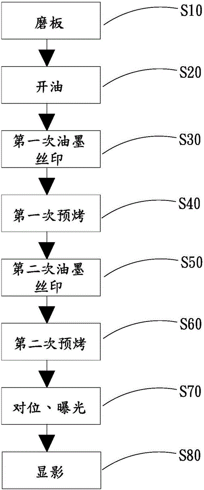
[0029] See attached figure 1 and figure 2 , which is a screen printing method for a thick copper printed circuit board according to an embodiment of the present invention.

[0030] Such as figure 1 As shown, the screen printing method of this kind of thick copper printed circuit board includes steps:

[0031] S10: Provide a printed circuit board 10 that has been electroplated and thickened with copper lines, and polish the printed circuit board 10 .

[0032] S20: Prepare the ink, and adjust the oil-opening viscosity of the ink to 50Pa·s˜80Pa·s. Preferably, the oil-ope...


PUM

PropertyMeasurementUnit
Widthaaaaaaaaaa
Widthaaaaaaaaaa

Abstract

The invention relates to a screen printing method of a thick copper printed circuit board. The method comprises the following steps of board polishing, oil mixing, first ink screen printing, first pre-baking, second ink screen printing, second pre-baking, alignment and exposure and developing. According to the screen printing method of the thick copper printed circuit board, twice ink screen printing is carried out. In the first ink screen printing, an ink ribbon surrounding a copper circuit is formed in a base material region and close to the edge of the copper circuit; and the ink ribbon is used for reducing the fall between the relatively thick copper circuit and the base material surface. In the second ink screen printing, coverage ink screen printing is carried out on a copper circuit region and a base material region. Through the method, the problem that the ink thickness on the edge of the copper circuit of the thick copper printed circuit board is not up to standard is solved; and the yield of a product is improved.

Description

technical field [0001] The invention relates to the technical field of printed circuit boards, in particular to a screen printing method for thick copper printed circuit boards. Background technique [0002] In the production process of printed circuit boards, the copper foil on the printed circuit board is etched into copper lines (forming the bottom copper layer) by etching process, and then electroplated to thicken the copper lines (forming an additional copper layer), and then a layer of The ink is coated on the circuit and substrate that do not need to be soldered on the printed circuit board, such as the green oil commonly used in the industry. Its function is: (1) to prevent the physical disconnection of the conductor circuit; (2) to prevent the Short circuit caused by bridging; (3) Solder only on the parts that must be soldered to avoid waste of solder; (4) Reduce copper pollution to the solder tank; (5) Prevent insulation deterioration caused by external environment...

Claims


Application Information

Patent Timeline
IPC IPC(8): H05K3/12H05K3/22
CPCH05K3/1216H05K3/227H05K2203/1476
Inventor 林瑞康刘维
Owner 东莞万钧电子科技有限公司
Why Eureka
Try Eureka