Sensor module and manufacturing method thereof
A sensor module, sensor chip technology, applied in the field of sensors
- Summary
- Abstract
- Description
- Claims
- Application Information
AI Technical Summary
Problems solved by technology
Method used
Image

Examples
Embodiment 1
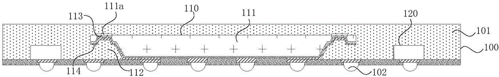
[0061] figure 1 It is a schematic structural diagram of the sensor module provided by Embodiment 1 of the present invention. The sensor module provided by the embodiment of the present invention may include an image sensor module, a fingerprint sensor module or other products, and may be applied to electronic devices such as smart phones, tablet computers, digital cameras, car driving recorders, attendance machines, and access control devices. The present invention is not limited thereto.
[0062] Such as figure 1 As shown, the sensor module provided in this embodiment includes:
[0063] The sensor chip 110 and at least one first auxiliary chip 120, the sensor chip 110 and at least one first auxiliary chip 120 are packaged into a chip package 100 by the plastic encapsulation material 101, and the circuit faces of the sensor chip 110 and at least one first auxiliary chip 1220 face the same direction;
[0064] Wherein, the sensor chip 110 includes a sensing unit 111, the sen...
Embodiment 2
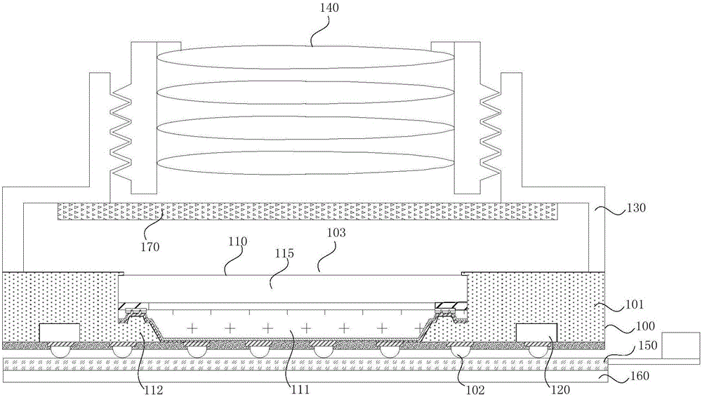
[0071] figure 2 It is a schematic structural diagram of the sensor module provided by Embodiment 2 of the present invention. Such as figure 2 As shown, further, the sensor chip is an image sensing chip 110, the image sensing chip 110 includes an image sensing unit 111, and a packaging glass 115 arranged above the light incident surface of the image sensing unit 111, and the front side of the chip package 100 is formed The light through hole 103 corresponding to the packaging glass 115, the back edge of the image sensing unit 111 is formed with a groove structure 112, and the image sensing unit 111 includes a welding pad opposite to the groove structure 111;
[0072] The sensor module also includes:
[0073] The lens holder 130 is installed on the front of the chip package 100, and the lens group 140 is fixed on the lens holder 130, and the lens group 140 includes at least one optical film.
[0074] Optionally, the molding material 101 covers the edge of the light incident...
Embodiment 3
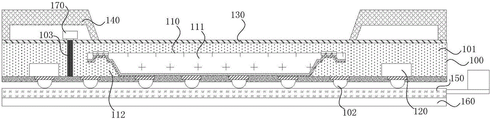
[0081] image 3 It is a schematic structural diagram of the sensor module provided by Embodiment 3 of the present invention. Such as image 3 As shown, further, the sensor chip is a fingerprint sensor chip 110, the fingerprint sensor chip 110 includes a fingerprint sensor unit 111, on the front of the chip package 100, the plastic packaging material 101 at least partially covers the working surface of the fingerprint sensor chip 110.
[0082] Optionally, the front surface of the chip package 100 is further provided with a color coating and / or a wear-resistant coating 130 .
[0083] Optionally, a protruding limiting ring 140 is provided on the front edge of the chip package 100 , and the area defined by the limiting ring 140 corresponds to the working surface of the fingerprint sensor chip 110 .
[0084] The sensor module provided in this embodiment also includes a rigid-flex board 150, wherein the rigid-flex board 150 includes a conductive circuit layer, and a plurality of w...
PUM
 Abstract
Description
Claims
Application Information
 - R&D
- Intellectual Property
- Life Sciences
- Materials
- Tech Scout
- Unparalleled Data Quality
- Higher Quality Content
- 60% Fewer Hallucinations
Browse by: Latest US Patents, China's latest patents, Technical Efficacy Thesaurus, Application Domain, Technology Topic, Popular Technical Reports.
© 2025 PatSnap. All rights reserved.Legal|Privacy policy|Modern Slavery Act Transparency Statement|Sitemap|About US| Contact US: help@patsnap.com