Terminal structure of super-junction MOS and manufacturing method thereof

A terminal structure and manufacturing method technology, applied in the direction of electrical components, circuits, semiconductor devices, etc., can solve the problems of reducing device stability and reliability, unstable device performance, complex and cumbersome processes, etc., to improve stability, simplify structure, damage reduction effect

Inactive Publication Date: 2016-12-14
SHANGHAI CHANGYUAN WAYON MICROELECTRONICS
View PDF3 Cites 5 Cited by
  • Summary
  • Abstract
  • Description
  • Claims
  • Application Information

AI Technical Summary

Problems solved by technology

[0004] For super-junction devices, the terminal protection technology is somewhat different from traditional DMOS. The terminal region of super-junction devices generally adopts an alternating structure of P-type pillars and N-type pillars similar to the active region, and then forms different fields on it. ring and field plate to protect the terminal electric field; in order to form alternate p-column regions and n-column regions with different aspect ratios in super junction devices, the process generally adopts multiple epitaxy, deep trench epitaxy and deep trench side injection. , the process is complicated and cumbersome, and it is easy to cause the instability of device performance
Generally speaking, the reasonable introduction of terminal protection structures such as field rings and field plates can make the distribution of the terminal electric field more uniform, which is conducive to the stability of the device voltage. In fact, in the P / N alternating structure of the super junction device terminal, The control of the field ring and the field plate is uncertain, which not only increases the complexity of the process, but also easily introduces certain impurity defects on the chip surface. The impurity defects will introduce some additional charges inside the device, thereby affecting the P / N in the terminal. The electric field effect of the type alternating structure reduces the stability and reliability of the device

Method used


Image

  • Terminal structure of super-junction MOS and manufacturing method thereof
  • Terminal structure of super-junction MOS and manufacturing method thereof
  • Terminal structure of super-junction MOS and manufacturing method thereof

Examples


Embodiment Construction

[0031] The present invention is described in detail below in conjunction with accompanying drawing and specific embodiment:

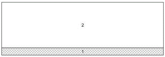
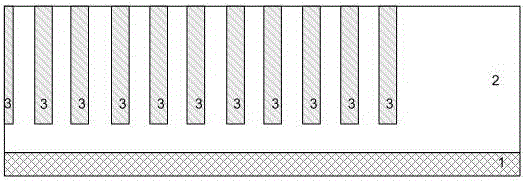
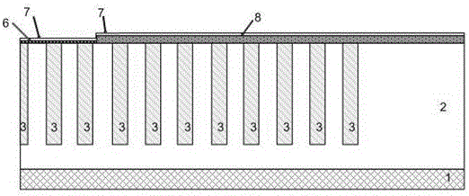
[0032] The terminal structure of a super junction MOS of the present invention includes P-type pillars and N-type pillars, wherein: a polycrystalline field plate 7 is used in the transition region from the active region to the terminal region to make the electric field distribution smoothly transition from the active region To the terminal area, the alternating structure of P-type columns and N-type columns in the terminal area is used to balance the electric field charge, wherein, the N-type epitaxial layer 2 is grown on the heavily doped N+ substrate 1, and the N-type epitaxial layer 2 An oxide layer is grown on the surface, and the trench in the active area and the trench ring in the terminal area are etched through the photolithography plate using deep groove etching. In this embodiment, the trench is a P-type trench 3, assuming that the trench width...


PUM


Abstract

The invention relates to a terminal structure of a super-junction MOS and a manufacturing method thereof. The terminal structure of the super-junction MOS comprises P-type columns and N-type columns; as a polycrystalline field plate is adopted by a transition region from an active region to a terminal region, electric field distribution is transited smoothly and steadily from the active region to the terminal region, and then electric field charges are balanced by utilizing a P-type column and N-type column alternating structure of the terminal region; an N-type epitaxial layer is grown on a heavily doped N+ substrate, an oxide layer is grown on the surface of the epitaxial layer, grooves of the active region and groove rings of the terminal region are etched through a photo-mask by utilizing trench etching; and if the width of the groove is a, the interval of the grooves of the active region is b and the interval of the grooves of the terminal region is c, c is greater than a but less than or equal to b. By simplifying the structure of the terminal region, the disadvantage of impurity introduction when other structures such as the polycrystalline field plate are introduced at a device terminal can be prevented. Meanwhile, damage to the device per se is reduced, and the stability of device performance is improved under the condition of not affecting the technology.

Description

technical field [0001] The invention relates to a terminal structure of a super junction MOS and a manufacturing method thereof, belonging to a terminal structure of a super junction power MOS device and a manufacturing method thereof. Background of the invention [0002] Super-junction power MOS is developed on the basis of ordinary DMOS technology. Compared with ordinary DMOS, in addition to the characteristics of high input impedance, fast switching speed, simple driving circuit, and high operating frequency, the most important thing is to overcome the traditional power MOS. theoretical limit. This structure uses alternating PN junction structure instead of low-doped drift region as the withstand voltage layer, and a lateral electric field is introduced in the drift region. In order to realize the mutual compensation of charges, the device drift region will be completely depleted, and the breakdown voltage is only as high as The thickness of the depletion layer is relate...

Claims


Application Information

Patent Timeline
Patent Type & Authority Applications(China)
IPC IPC(8): H01L29/06H01L29/40H01L29/78
CPCH01L29/0603H01L29/402H01L29/78
Inventor 任杰
Owner SHANGHAI CHANGYUAN WAYON MICROELECTRONICS
Why Eureka
Try Eureka