Supercharge Your Innovation With Domain-Expert AI Agents!

Semiconductor device with reduced emitter efficiency

A semiconductor, device technology, applied in the field of semiconductor devices with reduced emitter efficiency

Active Publication Date: 2016-12-21
INFINEON TECH AG
View PDF5 Cites 1 Cited by
  • Summary
  • Abstract
  • Description
  • Claims
  • Application Information

AI Technical Summary

Problems solved by technology

For example, in a reverse conducting IGBT, the switching losses due to the reverse recovery of the monolithically integrated diode can be reduced by reducing the anode efficiency of the monolithically integrated diode

Method used


Image

  • Semiconductor device with reduced emitter efficiency
  • Semiconductor device with reduced emitter efficiency
  • Semiconductor device with reduced emitter efficiency

Examples


Embodiment Construction

[0033] In the following Detailed Description, reference is made to the accompanying drawings, which form a part hereof, and which are shown by way of illustration of specific embodiments in which the invention may be practiced.

[0034] In this regard, directional terms such as "top", "bottom", "below", "front", "rear", "back", "primary", "rear", etc. may refer to the described Use the directions of the attached drawings. Since portions of an embodiment may be oriented in a number of different orientations, directional terms are used for purposes of illustration and are not limiting in any way. It is to be understood that other embodiments may be utilized and structural or logical changes may be made without departing from the scope of the present invention. Accordingly, the following detailed description is not taken in a limiting sense, and the scope of the invention is defined by the appended claims.

[0035] Reference will now be made in detail to various embodiments, on...


PUM


Abstract

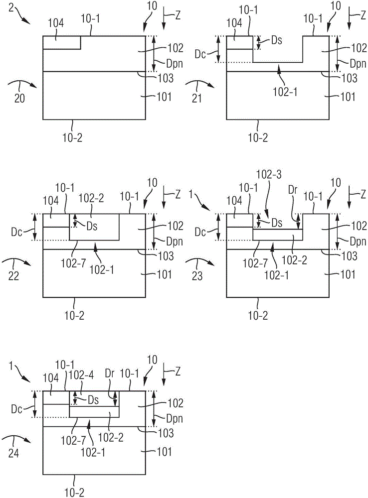
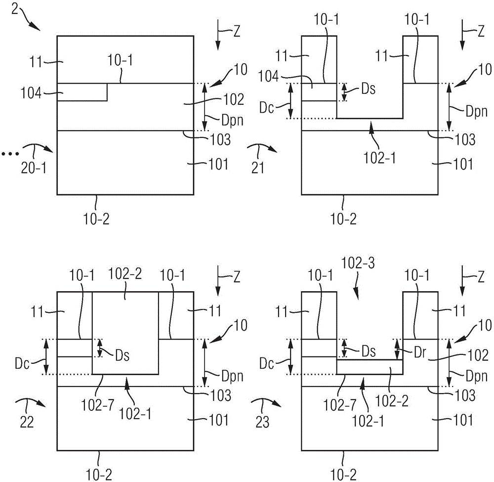
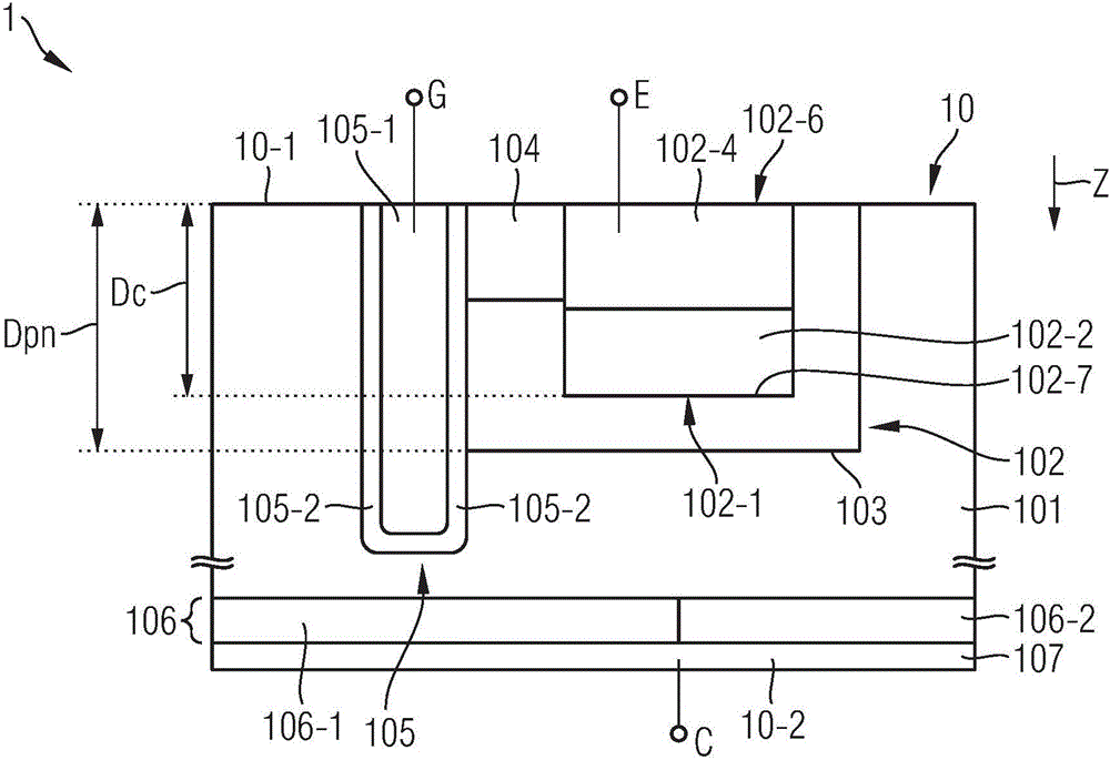
The invention relates to a semiconductor device with reduced emitter efficiency. A method of producing a semiconductor device (1) includes providing (20) a semiconductor body (10) having a front side (10-1) and a back side (10-2), wherein the semiconductor body (10) includes a drift region (101) having dopants of a first conductivity type and a body region (102) having dopants of a second conductivity type complementary to the first conductivity type, a transition between the drift region (101) and the body region (102) forming a pn-junction. The method further comprises: creating (21) a contact groove (102-1) in the semiconductor body (10), the contact groove (102-1) extending into the body region along a vertical direction (Z) pointing from the front side (10-1) to the back side (10-2); and filling (22) the contact groove (102-1) at least partially by epitaxially growing a semiconductor material within the contact groove (102-1), wherein the semiconductor material (102-2) has dopants of the second conductivity type.

Description

technical field [0001] The present description relates to embodiments of methods for manufacturing semiconductor devices and to embodiments of semiconductor devices. In particular, the present description relates to embodiments of methods for fabricating semiconductor devices with reduced emitter efficiency and to corresponding embodiments of semiconductor devices. Background technique [0002] Many functions of modern devices in automotive, consumer and industrial applications, such as converting electrical energy and driving electric motors or motors, rely on semiconductor devices. For example, insulated gate bipolar transistors (IGBTs), metal oxide semiconductor field effect transistors (MOSFETs), and diodes have been used in various applications including, but not limited to, switches in power supplies and power converters. [0003] At times, it may be desirable to provide such power semiconductor devices with reduced emitter efficiency in order to minimize switching lo...

Claims


Application Information

Patent Timeline
Patent Type & Authority Applications(China)
IPC IPC(8): H01L29/739H01L29/06H01L21/331
CPCH01L29/1095H01L29/0834H01L29/41766H01L29/4236H01L29/66348H01L29/66734H01L29/7397H01L29/7813H01L29/861H01L29/8613H01L29/7395H01L29/0603H01L29/66333
Inventor J·鲍姆加特尔V·科马尔尼茨基W·瓦格纳
Owner INFINEON TECH AG
Features
  • R&D
  • Intellectual Property
  • Life Sciences
  • Materials
  • Tech Scout
  • Unparalleled Data Quality
  • Higher Quality Content
  • 60% Fewer Hallucinations
Learn More