Method for processing touch screen conductive glass with double-side shadow elimination
A technology of conductive glass and processing methods, applied in glass manufacturing equipment, glass cutting devices, manufacturing tools, etc., can solve the problems of viewing pattern influence, influence electromagnetic shielding, electrostatic protection function, etc., to achieve high uniformity, good electromagnetic shielding, The effect of low energy consumption
- Summary
- Abstract
- Description
- Claims
- Application Information
AI Technical Summary
Problems solved by technology
Method used
Image
Examples
Embodiment 1
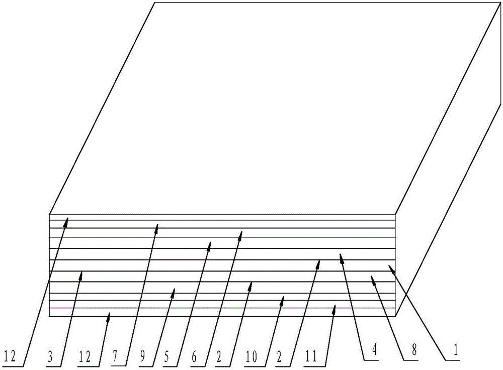
[0027] Both surfaces of the upper glass substrate 1 and the lower glass substrate 8 are the tin surface 2 and the air surface 3, and the air surfaces 3 of the upper glass substrate 1 and the lower glass substrate 8 are correspondingly bonded, and the tin surface 2 on the upper surface of the upper glass substrate 1 is An upper transparent layer 1 4 is arranged above, an upper transparent passivation layer 5 is arranged between the upper transparent layer 1 4 and the upper transparent layer 2 6, an upper interference layer 7 is arranged above the upper transparent layer 2 6, and an ITO film 12 is arranged above the upper interference layer 7 A lower interference layer 9 is arranged under the tin surface 2 on the lower surface of the lower glass substrate 8, a lower transparent passivation layer 10 is arranged between the lower interference layer 9 and the lower transparent layer 11, and an ITO film 12 is arranged under the lower transparent layer 11;
[0028] Both the upper tran...
Embodiment 2
[0031] In the first step, the upper glass substrate 1 and the lower glass substrate 8 are processed,
[0032] A. Cutting the upper glass substrate 1 and the lower glass substrate 8, first X cutting, then Y cutting, and then breaking into pieces;
[0033] B. Carry out edging and chamfering on the cut upper glass substrate 1 and lower glass substrate 8, first X edging, then chamfering, rotate 90° and then Y edging and chamfering;
[0034] C. Scrub and dry;
[0035] D, polishing the upper glass substrate 1 and the lower glass substrate 8 after edging and chamfering;
[0036] E, then brush and dry;
[0037] In the second step, the upper transparent layer 1 4, the upper transparent passivation layer 5, the upper transparent layer 2 6, the lower interference layer 9, and the lower transparent passivation layer 10 are sputtered on the upper glass substrate 1 and the lower glass substrate 8;
[0038] A. After polishing, brushing and drying, the upper glass substrate 1 and the lower...
PUM
 Abstract
Description
Claims
Application Information
