

Super-junction device manufacturing method and super-junction device
A superjunction device and epitaxial layer technology, which is applied in semiconductor/solid-state device manufacturing, semiconductor devices, electrical components, etc., can solve problems such as large gate-to-drain capacitance, reduce gate-to-drain capacitance, reduce switching loss, and reduce switching time. Effect
- Summary
- Abstract
- Description
- Claims
- Application Information
AI Technical Summary
Problems solved by technology
Method used
Image

Examples
Embodiment 1
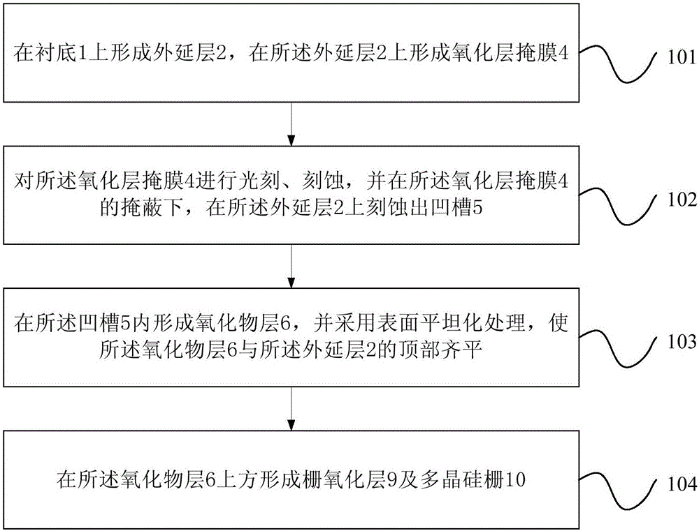
[0043] Embodiment 1 of the present invention provides a method for manufacturing a super junction device. figure 1 A flow chart of the method for manufacturing a super junction device provided in this embodiment. Such as figure 1 As shown, the method for manufacturing a super junction device in this embodiment may include:
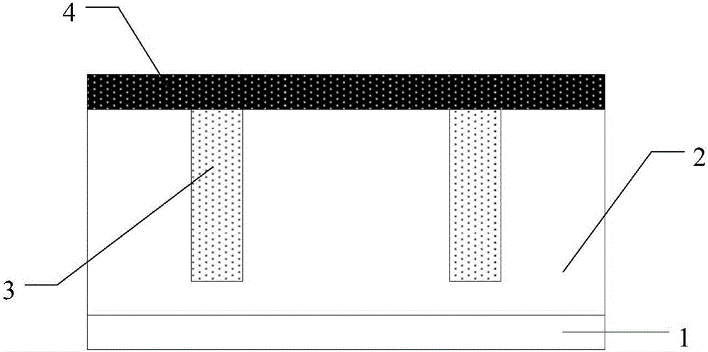
[0044] Step 101 , forming an epitaxial layer 2 on the substrate 1 , and forming an oxide layer mask 4 on the epitaxial layer 2 .
[0045] Specifically, the epitaxial layer 2 in this embodiment can be an N-type epitaxial layer, and the substrate 1 can be an N-type substrate. The method for forming the N-type epitaxial layer and the N-type substrate belongs to the prior art, and is not described in this embodiment. Let me repeat.
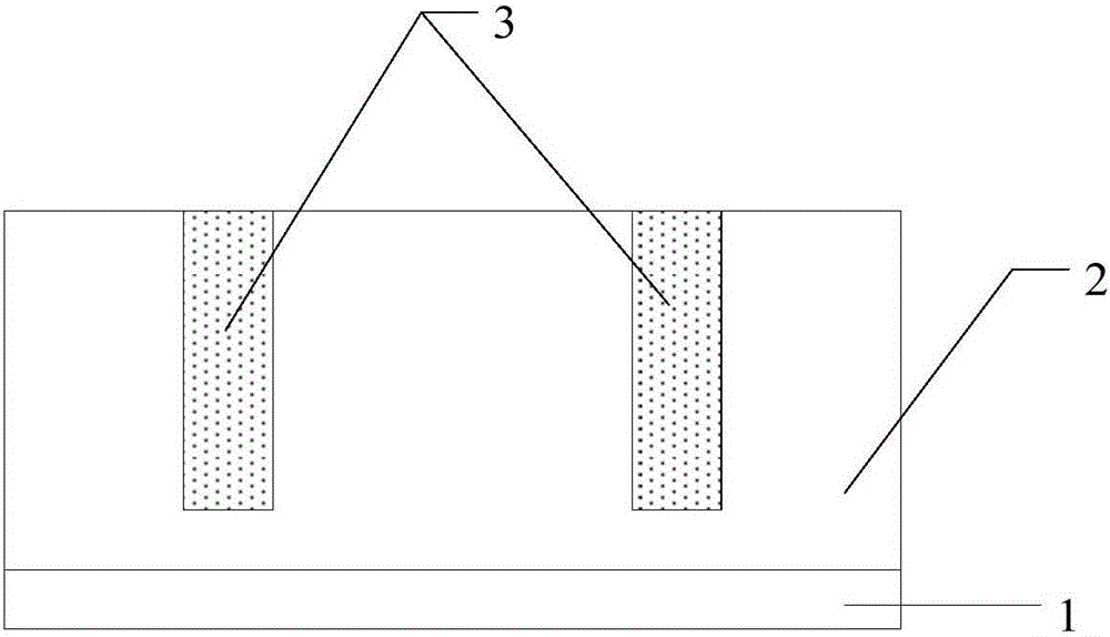
[0046] The method provided in this embodiment, after forming the epitaxial layer 2 on the substrate 1 and before forming the oxide layer mask 4 on the epitaxial layer 2, may further include: forming a super junction P column in...
Embodiment 2
[0060] Embodiment 2 of the present invention provides a super junction device. For the super device provided in this embodiment, please refer to Figure 10 . Such as Figure 10 As shown, the super junction device in this embodiment may include: a substrate 1, an epitaxial layer 2 formed on the substrate 1, an oxide layer 6, and a gate oxide layer formed on the oxide layer 6 9, and a polysilicon gate 10 formed on the gate oxide layer 9;
[0061] Wherein, the epitaxial layer 2 is provided with a groove 5 , the oxide layer 6 is located in the groove 5 , and the oxide layer 6 is flush with the top of the epitaxial layer 2 .
[0062] Specifically, the epitaxial layer 2 may be an N-type epitaxial layer. Correspondingly, the super-junction device in this embodiment may further include: a super-junction P-column structure 3 formed in the epitaxial layer 2, a P-type body Region 7, N-type source region 8, and dielectric layer 11 and metal layer 12 formed on the polysilicon gate 10. ...
PUM
 Abstract
Description
Claims
Application Information