Storage member and manufacture method

A technology for storage elements and manufacturing methods, applied in semiconductor/solid-state device manufacturing, electrical components, electric solid-state devices, etc., can solve problems affecting the performance of memory cells or memory cell arrays, and achieve the effects of avoiding programming interference and improving performance

Active Publication Date: 2017-01-04
MACRONIX INT CO LTD
View PDF6 Cites 2 Cited by
  • Summary
  • Abstract
  • Description
  • Claims
  • Application Information

AI Technical Summary

Problems solved by technology

[0003] However, as the size of the storage device becomes smaller and the integration level increases, the capacitance effect between the word line and the bit line becomes more and more obvious, and the program disturbance caused by it may affect the storage device. performance of a cell or memory cell array

Method used


Image

  • Storage member and manufacture method
  • Storage member and manufacture method
  • Storage member and manufacture method

Examples


Embodiment Construction

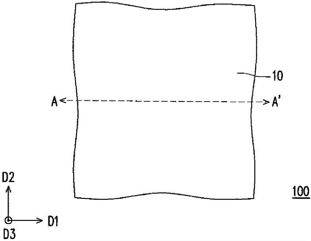
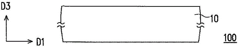
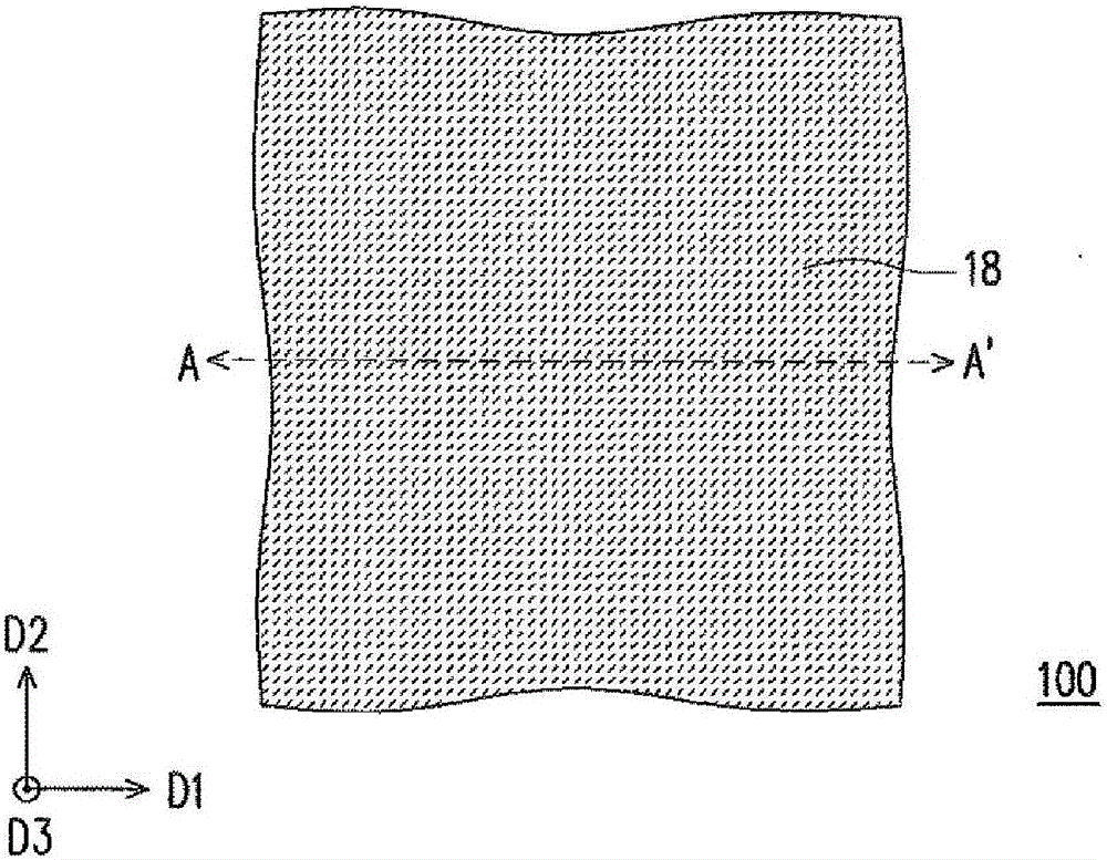
[0042] Figure 1A to Figure 1G It is a top view of a manufacturing method of a memory device according to an embodiment of the present invention. Figure 2A to Figure 2G for respectively along Figure 1A to Figure 1G The schematic cross-sectional view of the manufacturing method of the memory element shown by the A-A' line.

[0043] Please also refer to Figure 1A and Figure 2A , the manufacturing method of the memory element 100. First a substrate 10 is provided. Substrate 10 may comprise a semiconductor material, an insulator material, a conductor material, or any combination thereof. The material of the substrate 10 is, for example, a material composed of at least one material selected from the group consisting of Si, Ge, SiGe, GaP, GaAs, SiC, SiGeC, InAs and InP, or any material suitable for the process of the present invention physical structure. The substrate 10 includes a single-layer structure or a multi-layer structure. In addition, a silicon on insulator (SOI)...


PUM


Abstract

The invention discloses a storage unit and a manufacture method. The storage member comprises a substrate, a plurality of lamination structures, a plurality of conducting columns, a plurality of charge storage layers and a plurality of third conductor layers; the lamination layer structures are arranged on the base; the lamination layer structures are arranged along a first direction and extended along a second direction, wherein each lamination structure comprises a plurality of conducting layers and a plurality of dielectric layers which are alternatively laminated along a third direction; each conducting column is arranged on the base between the two adjacent lamination structures; each charge storage layer is positioned between the lamination layer structure and the conducting column; each third conducting layer is extended along the first direction, is intersected with the lamination structures in multiple intersection areas and covers part of the lamination structures and the tops of the conducting columns; and each intersection area of the lamination structure and the third conducting layer has an air gap and the air gap is extended along a third direction.

Description

technical field [0001] The present invention relates to a semiconductor element and its manufacturing method, and in particular to a memory element and its manufacturing method. Background technique [0002] As technology advances with each passing day, advances in electronic components have increased the need for greater storage capacity. To increase storage capacity, memory elements have become smaller and more densely packed. Therefore, the three-dimensional memory element has gradually drawn great attention from the industry. [0003] However, as the size of the storage device becomes smaller and the integration level increases, the capacitance effect between the word line and the bit line becomes more and more obvious, and the program disturbance caused by it may affect the storage device. performance of a cell or memory cell array. Therefore, how to reduce the capacitive effect between the word line and the bit line, so as to avoid the interference phenomenon caused...

Claims


Application Information

Patent Timeline
Patent Type & Authority Applications(China)
IPC IPC(8): H01L27/115H01L21/8247
Inventor 吴冠纬张耀文杨怡箴卢道政
Owner MACRONIX INT CO LTD
Why Eureka
Try Eureka