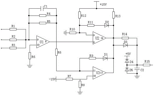
Grounding fault detecting circuit
A technology for detecting circuit and grounding faults, applied in the direction of measuring electricity, measuring electrical variables, measuring devices, etc., can solve the problems of disappearance of grounding phenomenon, false grounding of no-load busbar, etc., to achieve the effect of sensitive use and simple operation
- Summary
- Abstract
- Description
- Claims
- Application Information
AI Technical Summary
Problems solved by technology
Method used
Image
Examples
Embodiment 1
[0028] A ground fault detection circuit, with a hardware structure designed for fault detection and analysis, has the characteristics of simple operation and sensitive use, such as figure 1 As shown, it is specially set up as the following structure: including a three-phase vector input circuit, a first-stage adder circuit, a first window comparison circuit, a second window comparison circuit, and a detection and alarm processing circuit. The three-phase vector input circuit and the first The first-stage adder circuit is connected, the first-stage adder circuit is connected with the first window comparison circuit and the second window comparison circuit respectively, and both the first window comparison circuit and the second window comparison circuit are connected with the detection alarm processing circuit; A resistor R14, a resistor R15, a diode D3, a diode D4, a diode D5 and a capacitor C2 are arranged in the detection alarm processing circuit, the first end of the resisto...
Embodiment 2
[0030] This embodiment is further optimized on the basis of the above-mentioned embodiments, further to better realize the present invention, such as figure 1 As shown, the following arrangement structure is adopted in particular: the first-stage adder circuit is provided with an integrated operational amplifier U1, a resistor R4, a resistor R5, a resistor R6 and a capacitor C1, and the resistor R4, the resistor R5 and the capacitor C1 are connected in parallel with each other, and One of the common terminals connected in parallel is connected to pin 9 of the integrated operational amplifier U1, and the other common terminal connected in parallel is connected to the second window comparison circuit through the resistor R6, and the 10 pin of the integrated operational amplifier U1 is grounded through the resistor R6. Pin 8 of the integrated operational amplifier U1 is connected with the first window comparison circuit.
Embodiment 3
[0032] This embodiment is further optimized on the basis of any of the above embodiments, further to better realize the present invention, such as figure 1 As shown, the following setting structure is adopted in particular: a resistor R10, a resistor R11, a resistor R12, a resistor R13, a diode D2 and an integrated operational amplifier U2 are arranged in the first window comparison circuit, and the 8 pins of the integrated operational amplifier U1 It is connected to the 8-pin of the integrated operational amplifier U2, the first end of the resistor R11 is connected to the second end of the resistor R12, the first end of the resistor R12 is connected to the first end of the resistor R13, and the second end of the resistor R13 is respectively It is connected with the cathode of diode D2, the first end of resistor R14 and the 14th pin of integrated operational amplifier U2, the positive electrode of diode D2 is connected with the second end of resistor R11, and the 9th pin of int...
PUM
 Abstract
Description
Claims
Application Information
 - R&D
- Intellectual Property
- Life Sciences
- Materials
- Tech Scout
- Unparalleled Data Quality
- Higher Quality Content
- 60% Fewer Hallucinations
Browse by: Latest US Patents, China's latest patents, Technical Efficacy Thesaurus, Application Domain, Technology Topic, Popular Technical Reports.
© 2025 PatSnap. All rights reserved.Legal|Privacy policy|Modern Slavery Act Transparency Statement|Sitemap|About US| Contact US: help@patsnap.com

