Method for manufacturing wafer type film resistor

A technology of thin film resistors and manufacturing methods, applied in the field of resistor manufacturing, can solve problems such as increased environmental pollution, easy deformation of the resistor layer, poor quality, etc.

Inactive Publication Date: 2017-01-11
旺詮股ふん
View PDF4 Cites 0 Cited by
  • Summary
  • Abstract
  • Description
  • Claims
  • Application Information

AI Technical Summary

Problems solved by technology

However, when depositing and forming the resistance layer in this way, the resistance layer is likely to be poor in quality because the pattern and size of the mask layer are easily deformed, and the mask layer must be removed by chemical or cleaning methods after sputtering. In addition, its waste liquid treatment will increase the pollution of the environment

Method used


Image

  • Method for manufacturing wafer type film resistor
  • Method for manufacturing wafer type film resistor
  • Method for manufacturing wafer type film resistor

Examples


Embodiment Construction

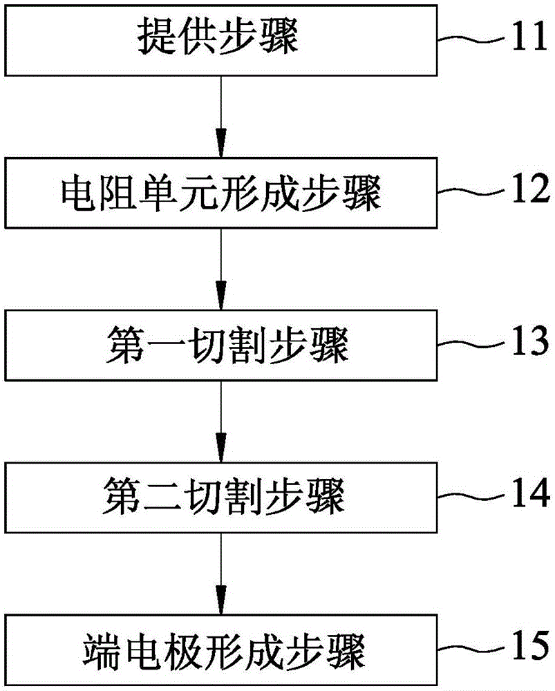
[0026] The present invention will be described in detail below in conjunction with the accompanying drawings and embodiments.

[0027] refer to figure 1 and figure 2 , a first embodiment of the manufacturing method of the chip-type thin film resistor of the present invention, comprising a providing step 11, a resistance unit forming step 12, a first cutting step 13, a second cutting step 14, and a terminal electrode forming step 15 .

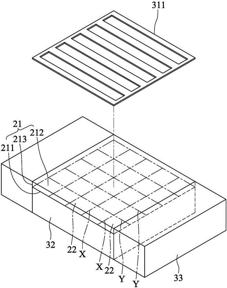
[0028] The providing step 11 is to provide a substrate 21, which includes a first surface 211, a second surface 212 opposite to the first surface 211, and a side connected to the first surface 211 and the second surface 212 213.

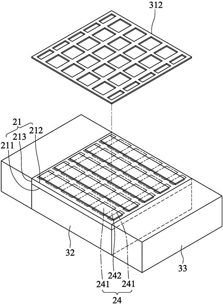
[0029] A plurality of first cutting lines X and a plurality of second cutting lines Y perpendicular to the first cutting lines X are defined from the first surface 211 of the substrate 21, wherein any pair of adjacent first, The second cutting lines X and Y jointly define a substrate unit 22 . Specifically, the f...


PUM


Abstract

A method for manufacturing a wafer type film resistor includes the following two steps: a providing step and a resistor unit forming step, a substrate is provided in the providing step, the substrate comprises a first surface and a second surface opposite to the first surface. The resistor unit forming step is as follows: preparing a magnetic mask having a predetermined pattern and a magnetic fixing member, and the magnetic mask and the magnetic fixing member are respectively arranged on the second surface and the first surface of the substrate, so that the magnetic mask is adsorbed and fixed on the second surface of the substrate through the magnetic fixing member, the magnetic mask masks the second surface of the substrate for sputtering for forming at least one resistor unit. In the process of sputtering deposition, the magnetic mask is attached to the substrate through the magnetic force effect so as to ensure that the shape and position of the formed resistor unit can be consistent with the accuracy.

Description

technical field [0001] The invention relates to a method for manufacturing a resistor, in particular to a method for manufacturing a chip type thin film resistor. Background technique [0002] The function of the resistor is to reduce the voltage and limit the current. Generally, chip resistors are divided into thick film resistors and chip thin film resistors. The film thickness of thick film resistors is generally greater than 5 μm, and most of them are produced by screen printing technology. The film thickness of thin film resistors is less than 1 μm, and most of them are produced by vacuum evaporation, magnetron sputtering and lithography etching of chemical deposition or physical deposition. [0003] In terms of the lithographic etching process, a resistive layer is firstly deposited on a substrate, and then a chip-type thin film resistor having a predetermined pattern of the resistive layer is formed using the lithographic etching process. However, the developer used ...

Claims


Application Information

Patent Timeline
IPC IPC(8): H01C17/12
Inventor 王万平
Owner 旺詮股ふん
Why Eureka
Try Eureka