Detection method of solder joint void defects based on laser pulse excitation simulation

A technology of laser pulse and defect detection, which is applied in the direction of material defect testing, special data processing applications, instruments, etc., can solve problems such as accurate preparation of solder joints, and achieve the effect of accurate judgment and simple operation

Active Publication Date: 2017-01-18
BEIJING INST OF SPACECRAFT ENVIRONMENT ENG
View PDF2 Cites 8 Cited by
  • Summary
  • Abstract
  • Description
  • Claims
  • Application Information

AI Technical Summary

Problems solved by technology

[0005] In fact, due to the inability to accurately prepare solder joints with fixed-size voids as required, the mapping relationship between the defect size of solder joint voids and the temperature distribution cannot be directly determined through experiments

Method used


Image

  • Detection method of solder joint void defects based on laser pulse excitation simulation
  • Detection method of solder joint void defects based on laser pulse excitation simulation
  • Detection method of solder joint void defects based on laser pulse excitation simulation

Examples


Embodiment Construction

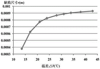
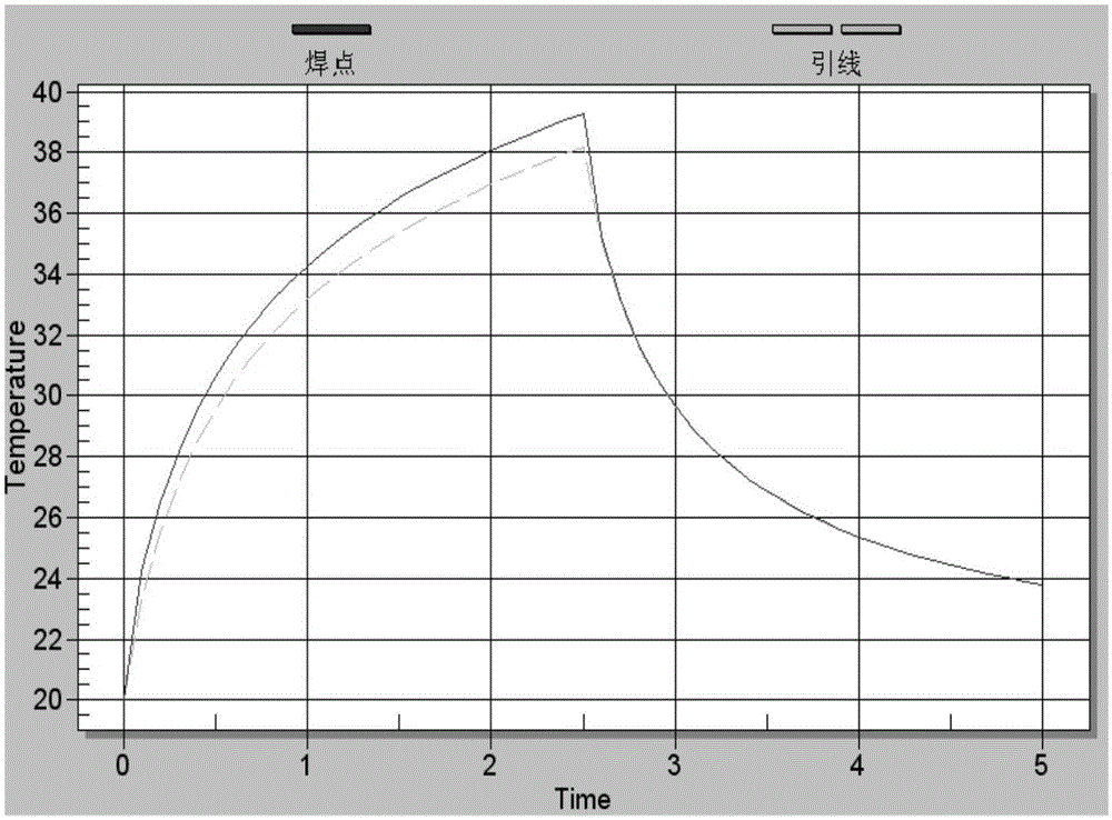
[0025] In order to illustrate the implementation of the present invention more clearly, the method of the present invention will be briefly introduced below in conjunction with the accompanying drawings. Obviously, the accompanying drawings in the following description are only some specific implementations of the present invention. For those of ordinary skill in the art Generally speaking, other drawings can also be obtained based on these drawings on the premise of not paying creative work.

[0026] The solder joint void defect detection method based on laser pulse excitation simulation of the present invention comprises the following steps:

[0027] (1) Establish a solder joint model that can quantify void defects

[0028] The Thermal Desktop thermal analysis software is embedded in the menu bar of AutoCAD software, and the two softwares are combined to establish a modeling and simulation analysis environment for solder joints. Through the combination of these two software...


PUM

PropertyMeasurementUnit
thermal conductivityaaaaaaaaaa

Abstract

The invention provides a detection method of solder joint void defects based on laser pulse excitation simulation, and can be used in the technical field of solder joint void defect screening, life prediction and evaluation and the like. According to the invention, a numerical solution algorithm is embedded into a solder joint heat conduction finite element model through a solder joint heat conduction finite element modeling method with the void defects and the numerical solution algorithm with void defect solder joint heat conduction problems and inverse problems under the conditions of the laser pulse constant heat flux density and natural convection excitation, so that a rule model of which the sizes of the solder joint void defects change along infrared temperature differences is established. Finally, on-line detection of the solder joint void defects is realized according to the rule model. The detection method disclosed by the invention is simple to operate and accurate in judgment and can be preliminarily used in actual production, and by adopting the detection method of the solder joint void defects, the detection rate of the solder joint void defects can reach nearly 100% in the case of artificial judgment.

Description

technical field [0001] The invention belongs to the technical fields of void defect screening, life prediction and evaluation of solder joints of electronic products. Specifically, the invention relates to a detection method of solder joint defects based on laser pulse excitation simulation. Background technique [0002] With the rapid development of electronic technology, electronic products have been applied to a wider range of fields, and people have put forward higher requirements for the quality and reliability of electronic products. In practice, there are many problems of failure of electronic products due to defects such as solder joint voids, virtual soldering, and cracks. The quality of solder joints is a key factor affecting the reliability of electronic products. Therefore, the inspection of the quality of solder joints of electronic products and the screening of defective products are the key to ensuring the reliability of products. [0003] Due to internal def...

Claims


Application Information

Patent Timeline
Patent Type & Authority Applications(China)
IPC IPC(8): G06F17/50G01N25/72
Inventor 黄小凯周月阁刘守文刘文根刘闯
Owner BEIJING INST OF SPACECRAFT ENVIRONMENT ENG
Why Eureka
Try Eureka