Absorption-rate-adjustable bandwidth electromagnetic wave absorber based on graphene film

A technology of graphene film and wave absorber, which is applied to electrical components, antennas, etc., can solve the problems of poor practicability and high cost, achieve the effects of reducing performance impact, reducing manufacturing difficulty and cost, and avoiding resource consumption

Active Publication Date: 2017-01-25
XIDIAN UNIV
View PDF3 Cites 28 Cited by
  • Summary
  • Abstract
  • Description
  • Claims
  • Application Information

AI Technical Summary

Problems solved by technology

[0004] The purpose of the present invention is to overcome the defects of the above-mentioned prior art, and propose a broadband electromagnetic absorber with adjustable absorption rate based on gra

Method used


Image

  • Absorption-rate-adjustable bandwidth electromagnetic wave absorber based on graphene film
  • Absorption-rate-adjustable bandwidth electromagnetic wave absorber based on graphene film
  • Absorption-rate-adjustable bandwidth electromagnetic wave absorber based on graphene film

Examples


Embodiment 1

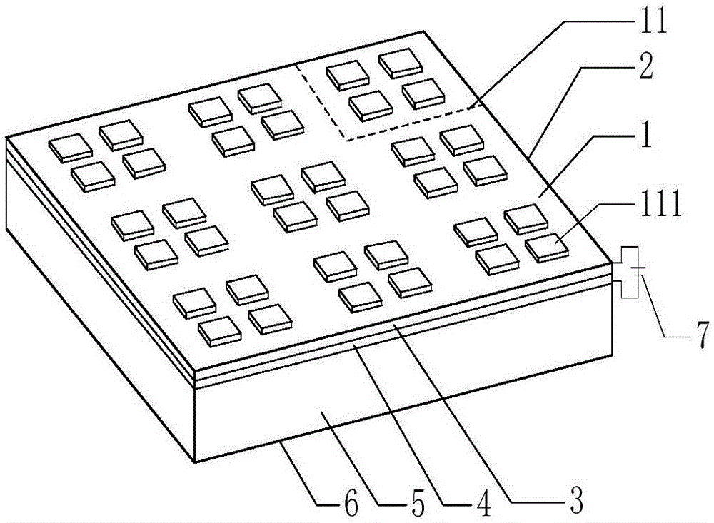
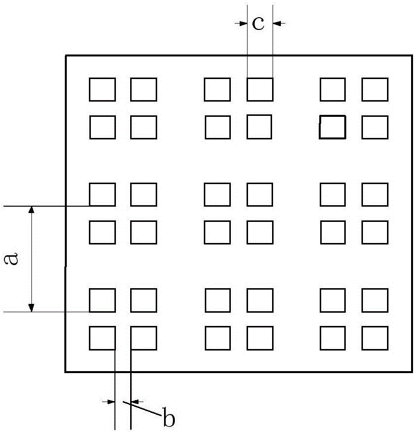
[0018] refer to figure 1 , a broadband electromagnetic absorber with adjustable absorption rate based on graphene film, including a conductive layer and a dielectric layer stacked up and down: the conductive layer includes a metal patch 1 and a graphene film attached to its lower surface 2. The metal patch 1 is etched with a plurality of cross-shaped slits of different forms to form M×N patch units 11, where M>2, N>2, and each patch unit 11 consists of m×n pieces Composed of patches 111, where m>2, n>2; the dielectric layer includes a first dielectric board 3, a second dielectric board 4 and a third dielectric board 5 stacked from top to bottom, wherein the first dielectric board 3 uses Insulating material, the second dielectric board 4 is made of semiconductor material; the bottom surface of the third dielectric board 5 is printed with a bottom board 6 . A DC power supply 7 is connected between the graphene film 2 and the second dielectric plate 4 for adjusting the surface c...

Embodiment 2

[0036] Embodiment 2 has the same structure as Embodiment 1, only the material of the third dielectric plate 5 and the relative permittivity ε r3 Made an adjustment: the third dielectric plate 5 selects the relative permittivity ε r3 4 polymethacrylate (PMMA) dielectric board.

Embodiment 3

[0038] Embodiment 3 has the same structure as Embodiment 1, only the material of the third dielectric plate 5 and the relative permittivity ε r3 Made an adjustment: the third dielectric plate 5 selects the relative permittivity ε r3 1.05 foam medium board.

[0039] Below in conjunction with simulation experiment, technical effect of the present invention is described further:

[0040] 1. Simulation conditions and content

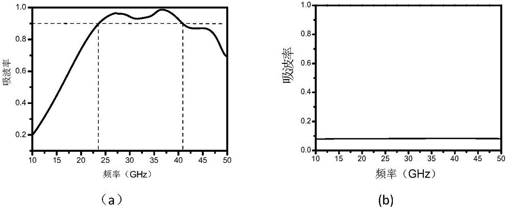
[0041] Utilize the commercial simulation software HFSS_13.0 to carry out the simulation calculation of the absorption rate curve of the wave absorber under different DC power supply voltages in the above-mentioned embodiment 1, the result is as follows image 3 shown.

[0042] 2. Simulation results

[0043] refer to image 3 , the abscissa in the figure is the frequency, the unit is GHz, the range is 10GHz-50GHz, and the ordinate indicates the normalized absorbed electromagnetic wave energy, the range is 0.1-1. from image 3 (a) It can be seen that th...


PUM

PropertyMeasurementUnit
Thicknessaaaaaaaaaa
Thicknessaaaaaaaaaa

Abstract

The invention provides an absorption-rate-adjustable bandwidth electromagnetic wave absorber based on a graphene film, and aims to solve the technical problems of high cost and poor practicability in the conventional absorption-rate-adjustable bandwidth electromagnetic wave absorber based on the graphene film. The absorption-rate-adjustable bandwidth electromagnetic wave absorber comprises a conductive layer and a dielectric layer which are laminated one above the other, wherein the conductive layer comprises a metal patch and a graphene film attached to the lower surface of the metal patch; a plurality of cross-shaped gaps of different forms are etched into the metal patch to form M*N patch units; each patch unit consists of m*n patches; the dielectric layer comprises a first dielectric plate, a second dielectric plate and a third dielectric plate which are laminated from top to bottom; a bottom plate is printed on the lower surface of the third dielectric plate; a direct-current power supply is connected between the graphene film and the second dielectric plate, and is used for adjusting surface conductivity of the graphene film. The absorption-rate-adjustable bandwidth electromagnetic wave absorber has the advantages of low cost and high practicability, and can be applied to occasions requiring an intermittent wave-absorbing feature such as a paraboloid antenna and an aircraft surface.

Description

technical field [0001] The invention belongs to the field of electromagnetic stealth technology, and relates to an adjustable broadband electromagnetic absorber, in particular to a graphene film-based broadband electromagnetic absorber with adjustable absorption rate, which can be used for electromagnetic wave absorbers in the field of adjustable absorption rate. Anti-interference and electromagnetic compatibility. Background technique [0002] Graphene is a two-dimensional planar carbon atom thin film material, which has the characteristics of single atomic layer thickness, high mechanical hardness, high carrier mobility, good flexibility and light transmission, and adjustable electrical conductivity. It can be used to design Various new nano-devices or transparent conductive materials, such as transparent electrodes, optical modulators, polarizers, plasmonic devices, photon detectors, superprisms and wave-absorbing devices, etc. [0003] Electromagnetic wave absorber or w...

Claims


Application Information

Patent Timeline
IPC IPC(8): H01Q17/00
CPCH01Q17/008
Inventor 吴边张兴飞赵雨桐苏雯薛宝玥
Owner XIDIAN UNIV
Why Eureka
Try Eureka