Transistor and formation method thereof

A technology of transistors and regions, applied in the direction of transistors, electric solid-state devices, semiconductor devices, etc., can solve problems such as unstable performance of SRAM, achieve performance improvement, weaken mismatch problems, and adjust accurately and stably

Active Publication Date: 2017-02-22
SEMICON MFG INT (SHANGHAI) CORP
View PDF6 Cites 5 Cited by
  • Summary
  • Abstract
  • Description
  • Claims
  • Application Information

AI Technical Summary

Problems solved by technology

[0006] However, due to the difference in work function layer materials required for PMOS transistors and NMOS transistors, the performance of the formed SRAM is unstable.

Method used


Image

  • Transistor and formation method thereof
  • Transistor and formation method thereof
  • Transistor and formation method thereof

Examples


Embodiment Construction

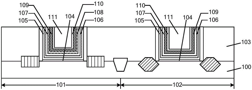
[0036]As mentioned in the background art, due to the difference in work function layer materials required by PMOS transistors and NMOS transistors, the performance of the formed SRAM is unstable.

[0037] After research, it is found that because the storage unit of the SRAM includes a PMOS transistor and an NMOS transistor, and the material of the work function layer required by the PMOS transistor and the NMOS transistor is different. In a PMOS transistor, a P-type work function material, such as TiN, is required between the gate layer and the gate dielectric layer; in an NMOS transistor, an N-type work function material, such as TiAl, is required between the gate layer and the gate dielectric layer. Since the N-type work function material usually has aluminum ions, and the particle size of the aluminum ions is small, the aluminum ions are easy to diffuse into the gate dielectric layer or even the substrate, resulting in changes in the performance of the transistor. Especiall...


PUM


Abstract

The invention provides a transistor and a formation method thereof. The formation method of the transistor comprises the steps that a substrate comprising a first region and a second region is provided; a dielectric layer is formed on the surface of the substrate, the dielectric layer of the first region is internally provided with a first opening, and the dielectric layer of the second region is internally provided with a second opening; a gate dielectric layer is formed on the surface of the dielectric layer, the side wall and the bottom surface of the first opening and the side wall and the bottom surface of the second opening; a cover layer is formed on the surface of the gate dielectric layer, wherein the material of the cover layer is first type of work function material; a first work function layer is formed on the surface of the cover layer of the first region, wherein the material of the first work function layer is the first type of work function material; a second work function layer is formed on the surface of the first work function layer and the surface of the cover layer of the second region, wherein the material of the second work function layer is second type of work function material; and a gate layer fully filling the first opening and the second opening is formed on the surface of the second work function layer. The mismatch problem between a PMOS transistor and an NMOS transistor can be improved.

Description

technical field [0001] The invention relates to the technical field of semiconductor manufacturing, in particular to a transistor and a forming method thereof. Background technique [0002] Static Random Access Memory (SRAM), as a member of memory, has the advantages of high speed, low power consumption and compatibility with standard processes, and is widely used in computers, personal communications, consumer electronics (smart cards, digital cameras, Multimedia player) and other fields. [0003] The storage unit of the SRAM includes a 4T (transistor) structure and a 6T (transistor) structure. For a 6T SRAM size unit, it includes: a first PMOS transistor P1 , a second PMOS transistor P2 , a first NMOS transistor N1 , a second NMOS transistor N2 , a third NMOS transistor N3 and a fourth NMOS transistor N4 . Wherein, the P1 and P2 are pull-up transistors; the N1 and N2 are pull-down transistors; and the N3 and N4 are transfer transistors. [0004] In the prior art, in ord...

Claims


Application Information

Patent Timeline
Patent Type & Authority Applications(China)
IPC IPC(8): H01L21/285H01L21/8238H01L27/092H01L27/11
CPCH01L27/092H01L21/28506H01L21/823842H10B10/12
Inventor 李勇
Owner SEMICON MFG INT (SHANGHAI) CORP
Why Eureka
Try Eureka