Array substrate and display device

A technology for array substrates and display devices, which is applied to semiconductor/solid-state device components, instruments, semiconductor devices, etc., and can solve problems such as cumbersomeness, life expectancy, and performance.

Active Publication Date: 2017-02-22
BOE TECH GRP CO LTD
View PDF3 Cites 8 Cited by
  • Summary
  • Abstract
  • Description
  • Claims
  • Application Information

AI Technical Summary

Problems solved by technology

Although the technical level of the etch barrier oxide array substrate has been mass-produced, due to the device reliability and reliability problems of the oxide array substrate, the current products have always had complex and cumbersome compensation methods (such as using

Method used


Image

  • Array substrate and display device
  • Array substrate and display device
  • Array substrate and display device

Examples


Embodiment 1

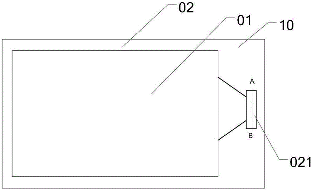
[0034] This embodiment provides an array substrate 10, such as image 3 As shown, it includes a display area 01 and a peripheral area 02 arranged on at least one side of the display area 01, image 3 A bonding area 021 located in the peripheral area 02 is also shown in . For example, bonding area 021 can be configured to connect external circuits. For example, the bonding area 021 can be configured to be connected with a driver IC, for example, can be used as a lead-out area of ​​a flexible circuit board.

[0035] Such as Figure 4 As shown, the array substrate includes a base substrate 101 and a first conductive layer 106 and a second conductive layer 110 sequentially arranged on the base substrate 101, and at least two conductive layers are arranged between the first conductive layer 106 and the second conductive layer 110 a passivation layer formed continuously in a direction perpendicular to the base substrate 101. A first conductive layer 106 , at least two passivatio...

Embodiment 2

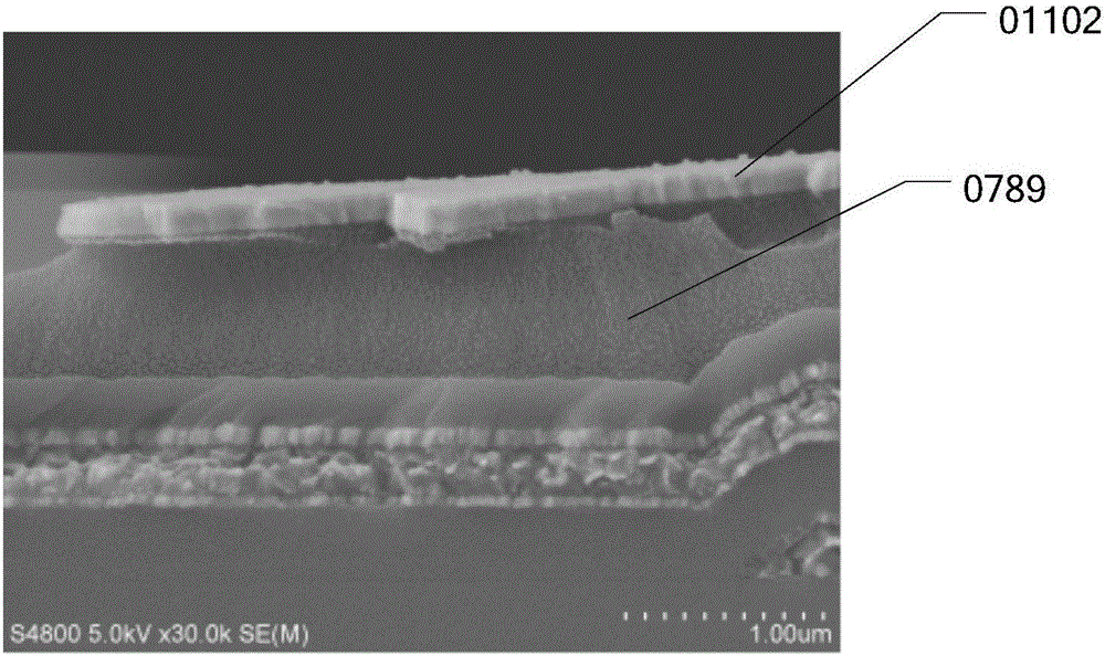
[0057] Different from the first embodiment, the first conductive layer 106 , at least two passivation layers and the second conductive layer 110 are only provided in the display area 01 . Can refer to Figure 6f Display area 01 on the left. The first conductive layer 106 includes a plurality of first conductive structures 1060 insulated from each other, and the first conductive structures 1060 can be source electrodes 1062 and drain electrodes 1061 . The second conductive layer 110 includes a plurality of second conductive structures 1102 insulated from each other, and the second conductive structures 1102 may be pixel electrodes. The second conductive structure 1102 may be electrically connected to the first conductive structure 1060 through via holes penetrating at least two passivation layers.

[0058] In one example, the second conductive structure 1102 can also be a common electrode. When the second conductive structure 1102 is a common electrode, the second conductive...

Embodiment 3

[0062] This embodiment provides a display device, including any one of the array substrates described in Embodiments 1 to 2.

[0063] For example, the display device includes a liquid crystal display device or an organic light emitting diode display device, but is not limited thereto.

[0064] For example, the display device may include display devices such as televisions, digital cameras, mobile phones, watches, tablet computers, notebook computers, and navigators.

[0065] The following description will be made by taking the display device as an example of a liquid crystal display device. When the display device is a liquid crystal display device, various modes such as ADS, HADS, TN, and VA can be used, which is not limited in this embodiment.

[0066] In an example, such as Figure 7As shown, the array substrate 10 and the opposite substrate 20 can be boxed together, and a liquid crystal layer (not shown in the figure) is formed therebetween, exposing the bonding region 0...


PUM


Abstract

The invention provides an array substrate and a display device. The array substrate comprises a substrate base plate, a first conductive layer and a second conductive layer successively arranged on the substrate base plate, wherein at least two continuously formed passivation layers which are vertical to the direction of the substrate base plate are arranged between the first conductive layer and the second conductive layer. The continuously formed passivation layers are arranged, so that the better adhesive property between the second conductive layer and the passivation layers in contact with the second conductive layer can be achieved by adjusting the components of the passivation layers and the connection performance between the layer and the layer is more stable. The continuously formed passivation layers are arranged, so that grooves can be conveniently formed in the passivation layers so as to increase the height difference of ACF glue non-electric connection area, the anisotropic conductive adhesive in the grooves is deformed or broken so as to increase the anisotropic conductivity of the anisotropic conductive adhesive and reduce the short circuit and/or open circuit of the display screen. Thus, the stability, reliability and dependability of the array substrate can be promoted.

Description

technical field [0001] At least one embodiment of the present disclosure relates to an array substrate and a display device. Background technique [0002] Large-scale oxide array substrates are currently in the stage of mass production and performance improvement, and mass-produced oxide array substrates basically have an Etching Stop Layer (ESL) structure. Although the technical level of the etch barrier oxide array substrate has been mass-produced, due to the device reliability and reliability problems of the oxide array substrate, the current products have always had complex and cumbersome compensation methods (such as using optical compensation, internal electrical compensation, External electrical compensation, etc.) and service life need to be improved, and the performance needs to be improved to apply to harsh environments, such as military products, high temperature, and humid environments. Contents of the invention [0003] At least one embodiment of the present ...

Claims


Application Information

Patent Timeline
IPC IPC(8): H01L27/12H01L27/32G02F1/1368
CPCG02F1/1368H01L27/1214H01L27/124H10K59/12H01L27/1248H01L27/1244H01L27/1225H01L29/66969H01L29/7869H10K59/124H01L23/3192H01L23/291H01L24/32H01L27/1262H01L21/02565H01L21/441G02F1/13452G02F1/136204G02F1/136286H01L2224/32225H01L2224/32145H01L23/3171G02F1/136295
Inventor 刘晓娣袁广才王刚
Owner BOE TECH GRP CO LTD
Why Eureka
Try Eureka