

OLED (Organic Light Emitting Diode) display panel and fabrication method
A technology for display panels and substrates, which is applied in semiconductor/solid-state device manufacturing, electrical components, and electric solid-state devices. The effect of improving color purity
- Summary
- Abstract
- Description
- Claims
- Application Information
AI Technical Summary
Problems solved by technology
Method used
Image

Examples
Embodiment Construction
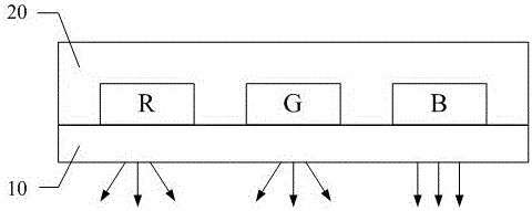
[0026] The present invention provides an OLED display panel and a manufacturing method. In order to make the purpose, technical solution and effect of the present invention clearer and more definite, the present invention will be further described in detail below. It should be understood that the specific embodiments described here are only used to explain the present invention, not to limit the present invention.
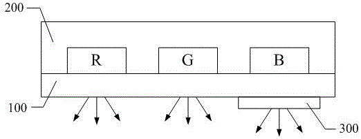
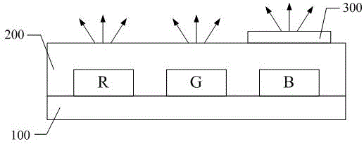
[0027] see figure 2 , figure 2 It is a schematic structural diagram of the first embodiment of an OLED display panel according to the present invention, which includes: a substrate 100, an OLED light-emitting device on the substrate 100, an encapsulation layer 200 encapsulated outside the OLED light-emitting device, and a light-scattering layer 300 , the OLED light-emitting device at least includes a red light-emitting device (R), a green light-emitting device (G) and a blue light-emitting device (B), wherein the blue light-emitting device adopts an optical micr...
PUM
| Property | Measurement | Unit |
|---|---|---|
| Diameter | aaaaa | aaaaa |
Abstract
Description
Claims
Application Information