Electronic assembly comprising a carrier structure made from a printed circuit board

A technology for printed circuit boards and load-bearing structures, applied in electronic components or electronic packages, in the field of manufacturing such electronic components, to achieve the effect of small engineering cost and firm mechanical attachment

Active Publication Date: 2017-03-01
AT & S AUSTRIA TECH & SYSTTECHN AG
View PDF6 Cites 7 Cited by
  • Summary
  • Abstract
  • Description
  • Claims
  • Application Information

AI Technical Summary

Problems solved by technology

[0007] Another problem to be solved is that many electronic products need to operate in an electrically noisy environment

Method used


Image

  • Electronic assembly comprising a carrier structure made from a printed circuit board
  • Electronic assembly comprising a carrier structure made from a printed circuit board
  • Electronic assembly comprising a carrier structure made from a printed circuit board

Examples


Embodiment Construction

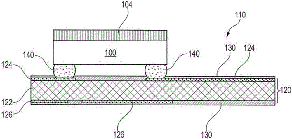
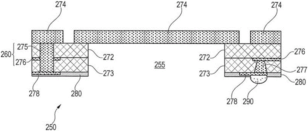
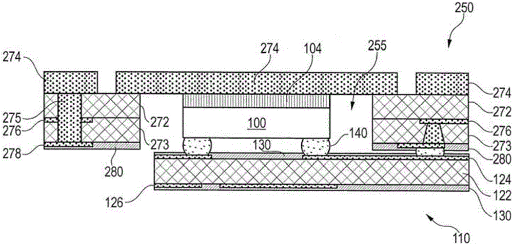
[0082] The illustrations in the figures are schematic. It is to be noted that in different figures, similar or identical elements or features are provided with the same reference signs. In order to avoid unnecessary repetition, elements or features which have already been explained with reference to the preceding figures will not be explained again later in the description.

[0083] Additionally, spatially relative terms such as "front" and "rear," "upper" and "lower," "left" and "right," etc., are used to describe one element's relationship to another as illustrated in the drawings. . Thus, spatially relative terms may be applied to orientations in use other than those depicted in the figures. Clearly, although all these spatially relative terms refer to the orientations shown in the figures, for ease of description and not necessarily as a limitation, devices according to embodiments of the present invention can, in use, assume orientations similar to those illustrated in ...


PUM


Abstract

In this document there is described an electronic assembly comprising (a) a base carrier structure (250) having a cavity (255) formed therein, (b) a cover carrier structure (110), and (c) an electronic component (100) being disposed within the cavity (255) and being connected electrically and / or thermally both with the cover carrier structure (110) and with the base carrier structure (250). The base carrier structure (250) is made at least partially from a printed circuit board (260). Preferably, also the cover carrier structure (110) is made at least partially from a further printed circuit board (120). It is further described an electronic device comprising such an electronic assembly and a method for manufacturing such an electronic assembly.

Description

technical field [0001] The present invention generally relates to the technical field of electronic components. In particular, the invention relates to electronic assemblies or electronic packages comprising mechanically protected and electrically connected electronic components, in particular semiconductor components or dies. The invention also relates to an electronic device comprising such an electronic component, and a method for manufacturing such an electronic component. Background technique [0002] The function of an electronic package is to protect sensitive electronic components, especially integrated semiconductor circuits, from harsh environmental influences without inhibiting electrical performance. Encapsulations are used to electrically and mechanically attach corresponding electronic components to desired electronic equipment or devices. [0003] A popular type of electronic package is the so-called Micro Leadframe Package (MLP), which is also known as Quad...

Claims


Application Information

Patent Timeline
Patent Type & Authority Applications(China)
IPC IPC(8): H01L23/498H01L23/538
CPCH01L23/49822H01L23/49833H01L23/5389H01L2224/16225H01L2224/73253H01L23/367H01L21/4857H01L21/52H01L23/3178H01L23/49811
Inventor 尼克·雷诺德·贝兹特
Owner AT & S AUSTRIA TECH & SYSTTECHN AG
Why Eureka
Try Eureka