Compound liquid crystal display device

A liquid crystal display device and composite technology, which is applied in the fields of instruments, computing, electrical and digital data processing, etc., can solve the problems of increasing cell thickness, insensitivity, and disturbing touch, and achieve the effect of increasing sensitivity and reducing cell thickness.

Inactive Publication Date: 2017-03-15
KUSN INFOVISION OPTOELECTRONICS
View PDF7 Cites 17 Cited by
  • Summary
  • Abstract
  • Description
  • Claims
  • Application Information

AI Technical Summary

Problems solved by technology

[0009] Since the touch box 116 currently used for the touch function is generally an external type, it needs to be attached to the liquid crystal box separately, which will increase the thickness of the box, and the viewing angle switching signal applied to the viewing angle control electrode 114 in the liquid crystal box will interfere with the touch control. , making it insensitive to

Method used


Image

  • Compound liquid crystal display device
  • Compound liquid crystal display device
  • Compound liquid crystal display device

Examples


no. 1 example

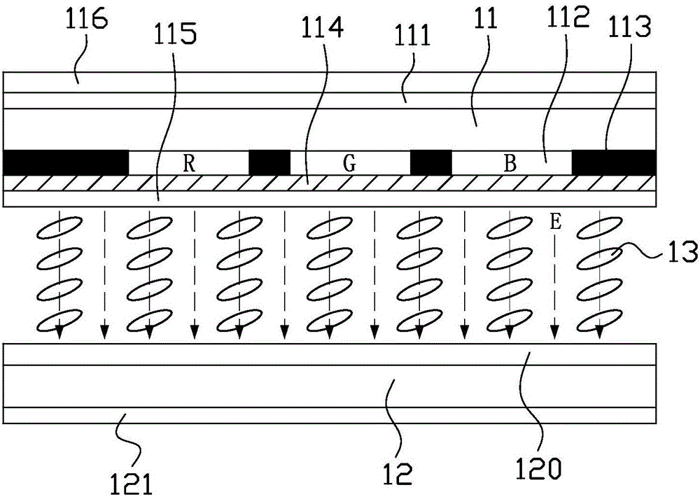
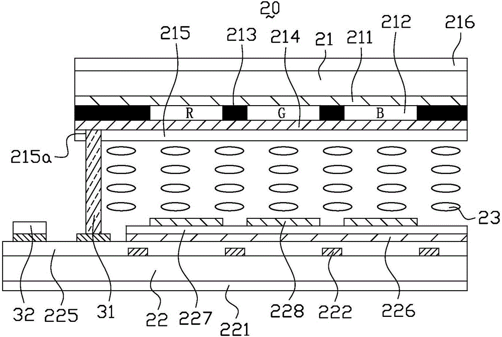
[0032] image 3 It is a schematic cross-sectional view of a liquid crystal display device at a wide viewing angle in the first embodiment of the present invention, Figure 4 for image 3 Schematic diagram of the cross-section of a liquid crystal display device at a narrow viewing angle, please refer to Figure 3 to Figure 4 The liquid crystal display device 20 provided in this embodiment includes a first substrate 21 , a second substrate 22 opposite to the first substrate 21 , and a liquid crystal layer 23 between the first substrate 21 and the second substrate 22 . Wherein, the first substrate 21 is a color filter substrate, and the second substrate 22 is a thin film transistor array substrate.

[0033] The liquid crystal display device 20 is an in-plane switching (IPS) liquid crystal display device using a horizontal electric field or a fringe field switching (FFS) liquid crystal display device using a fringe electric field. For IPS-type or FFS-type liquid crystal display...

no. 2 example

[0052] Figure 6 It is a schematic cross-sectional view of the liquid crystal display device in the second embodiment of the present invention, please refer to Figure 6 The main difference between this embodiment and the above-mentioned first embodiment is that, in this embodiment, a touch circuit layer 216, an insulating spacer layer 217, a second A polarizer 211 , a color resist layer 212 , a black matrix (BM) 213 , a viewing angle control electrode 214 and a flat layer 215 .

[0053] The touch circuit layer 216 is disposed on the inner surface of the first substrate 21 . The insulating spacer layer 217 is disposed on the touch circuit layer 216 . The first polarizer 211 is disposed on the insulating spacer layer 217 , that is, the touch circuit layer 216 is separated from the first polarizer 211 by the insulating spacer 217 . The first polarizer 211 is made of a metal material, and the first polarizer 211 can be formed specifically by using a metal wire grid process or ...

no. 3 example

[0057] Figure 7 It is a schematic cross-sectional view of the liquid crystal display device in the third embodiment of the present invention, please refer to Figure 7The main difference between this embodiment and the above-mentioned second embodiment is that in this embodiment, the order of the insulating spacer layer 217, the color resist layer 212 and the black matrix 213 is interchanged, that is, the touch circuit layer 216 is arranged on the first On the inner surface of the substrate 21 , for example, the touch circuit layer 216 is directly formed on the inner surface of the first substrate 21 . The color resist layer 212 and the black matrix 213 are staggered and disposed on the touch circuit layer 216 . The first polarizer 211 is disposed on the color resist layer 212 and the black matrix 213 , that is, the touch circuit layer 216 and the first polarizer 211 are separated by the color resist layer 212 and the black matrix 213 . The insulating spacer layer 217 is di...


PUM


Abstract

The invention provides a compound liquid crystal display device, comprising a first basal plate, a second basal plate arranged opposite to the first basal plate, and a liquid crystal layer located between the first basal plate and the second basal plate; the inner side of the first basal plate is provided with a first polaroid, a color-resisting layer, black matrixes and a viewpoint control electrode, the outer side or the inner side of the first basal plate is provided with a touch control circuit layer, the position of the first polaroid is located between the touch control circuit layer and the viewpoint control electrode, and the first polaroid is made of a metal material. The compound liquid crystal display device is additionally provided with a touch control function and a viewpoint switching function, box thickness does not need to be increased additionally, furthermore, interference of a viewpoint switching signal to touch control is reduced, so that the touch control is more sensitive.

Description

technical field [0001] The invention relates to the technical field of liquid crystal display, in particular to a composite liquid crystal display device. Background technique [0002] Liquid crystal display (liquid crystal display, LCD) has the advantages of good image quality, small size, light weight, low driving voltage, low power consumption, no radiation and relatively low manufacturing cost, and occupies a dominant position in the field of flat panel display. The liquid crystal display device includes a color filter substrate and a thin film transistor array substrate oppositely arranged, and a liquid crystal layer sandwiched between them. [0003] Currently, liquid crystal display devices are gradually developing toward wide viewing angles. For example, liquid crystal display devices using in-plane switching (IPS) or fringe field switching (FFS) modes can achieve wider viewing angles. However, in today's society, people pay more and more attention to protecting thei...

Claims


Application Information

Patent Timeline
Patent Type & Authority Applications(China)
IPC IPC(8): G02F1/1333G02F1/1335G06F3/041
CPCG02F1/13338G02F1/133528G06F3/0412G02F1/133531
Inventor 许雅琴
Owner KUSN INFOVISION OPTOELECTRONICS
Why Eureka
Try Eureka