Map correction method of mask, mask and manufacturing method of mask

A mask and layout technology, applied in the semiconductor field, can solve the problems of high mask scrap rate and inability to adjust etching parameters, etc.

Inactive Publication Date: 2017-03-15
SEMICON MFG INT (SHANGHAI) CORP +1
View PDF6 Cites 2 Cited by
  • Summary
  • Abstract
  • Description
  • Claims
  • Application Information

AI Technical Summary

Problems solved by technology

But for severely uneven distribution, such as figure 1 In the situation shown in , there is usually no good solution, because only one layer of the photomask is produced for the product layer structure, and it is impossible to adjust the etching parameters through trial and error like a wafer, so the scrap rate of this type of photomask will be very high

Method used


Image

  • Map correction method of mask, mask and manufacturing method of mask
  • Map correction method of mask, mask and manufacturing method of mask
  • Map correction method of mask, mask and manufacturing method of mask

Examples


Embodiment Construction

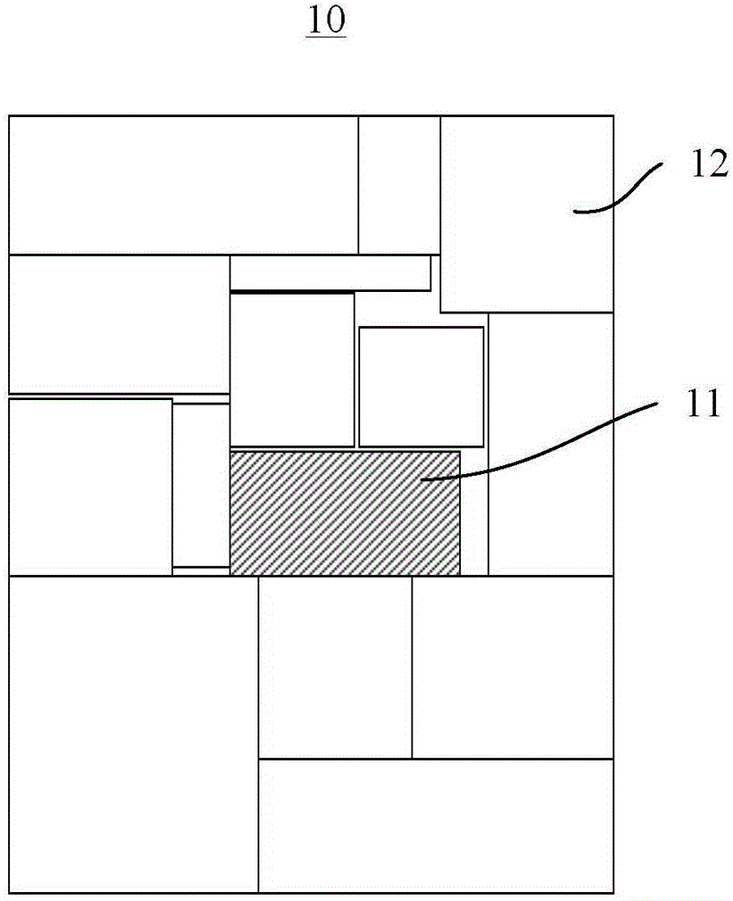
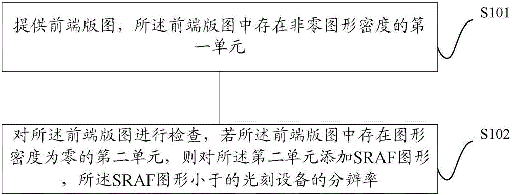
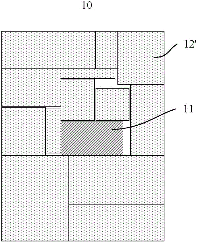
[0026] The layout modification method of the mask plate, the mask plate and its manufacturing method of the present invention will be described in more detail below in conjunction with the schematic diagrams, wherein a preferred embodiment of the present invention is shown, and it should be understood that those skilled in the art can modify the method described here the present invention while still achieving the advantageous effects of the present invention. Therefore, the following description should be understood as the broad knowledge of those skilled in the art, but not as a limitation of the present invention.

[0027] In the following paragraphs the invention is described more specifically by way of example with reference to the accompanying drawings. Advantages and features of the present invention will be apparent from the following description and claims. It should be noted that all the drawings are in a very simplified form and use imprecise scales, and are only u...


PUM

PropertyMeasurementUnit
widthaaaaaaaaaa
widthaaaaaaaaaa

Abstract

The invention discloses a map correction method of a mask, the mask and a manufacturing method of the mask. The map correction method of the mask disclosed by the invention comprises the steps as follows: a front-end map is provided and a first unit with non-zero graphic density exists in the front-end map; and the front-end map is inspected, if a second unit with zero graphic density exists in the front-end map, an SRAF graph is added to the second unit and the resolution ratio of the SRAF graph is smaller than that of lithography equipment. Compared with the prior art, the map correction method has the advantages that the graphic density of each unit can become closer after the SRAF graph is added, so that the overall graphic density of a photomask can become uniform by the further obtained mask, the yield of the photomask is improved and scrapping is basically avoided.

Description

technical field [0001] The invention relates to the technical field of semiconductors, in particular to a layout correction method of a mask, a mask and a manufacturing method thereof. Background technique [0002] MPW (Multi-Project Wafer, multi-project wafer) is to put multiple integrated circuit designs with the same process on the same wafer, and share the cost of tape-out according to the area, so as to reduce development costs and new product development risks, and reduce the risk of small and medium-sized wafers. The threshold for integrated circuit design companies at the start, reducing the serious waste of resources caused by a single test tape-out. [0003] The mask of an MPW is usually shared by multiple customers, and the products of these customers will have different degrees of difference in the manufacturing process. For example, in some ion implantation processes, some customers need to produce masks, some customers do not produce masks, and there are even ...

Claims


Application Information

Patent Timeline
Patent Type & Authority Applications(China)
IPC IPC(8): G03F1/36
Inventor 张士健郁志芳刘丽戴文旗徐佳明
Owner SEMICON MFG INT (SHANGHAI) CORP
Why Eureka
Try Eureka