CMOS image sensor structure with crosstalk improvement

A technology of lattice structure and reflective structure, applied in the field of semiconductor devices and their manufacturing, can solve the problem that the method of BSICMOS image sensor cannot fully meet the requirements and the like

Active Publication Date: 2017-03-22
TAIWAN SEMICON MFG CO LTD
View PDF3 Cites 11 Cited by
  • Summary
  • Abstract
  • Description
  • Claims
  • Application Information

AI Technical Summary

Problems solved by technology

[0004] However, conventional BSI CMOS image sensors and methods of manufacturing BSI CMOS image sensors cannot fully meet the requirements in every aspect

Method used


Image

  • CMOS image sensor structure with crosstalk improvement
  • CMOS image sensor structure with crosstalk improvement
  • CMOS image sensor structure with crosstalk improvement

Examples


Embodiment Construction

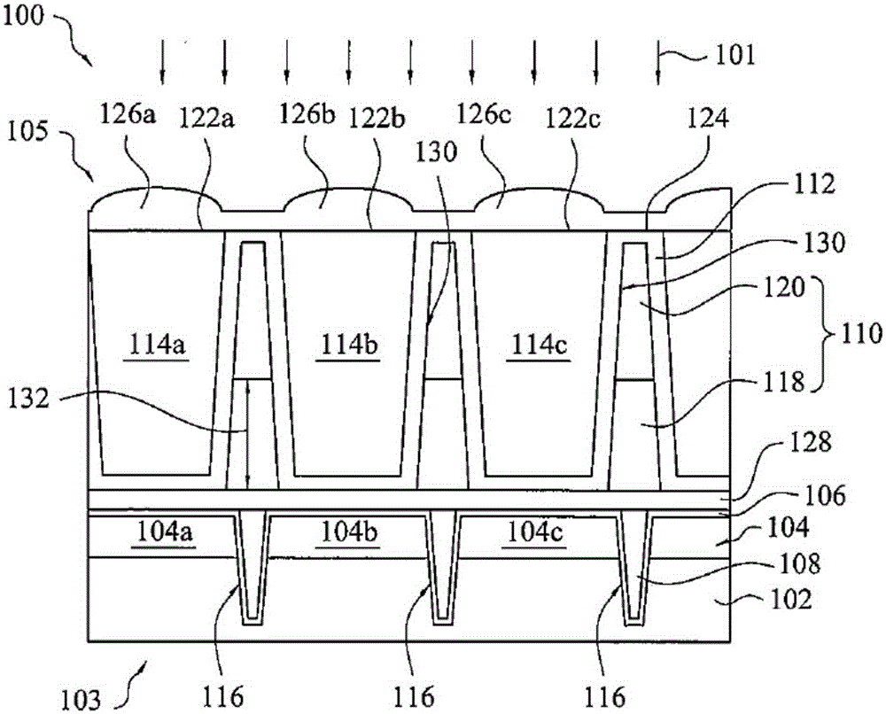
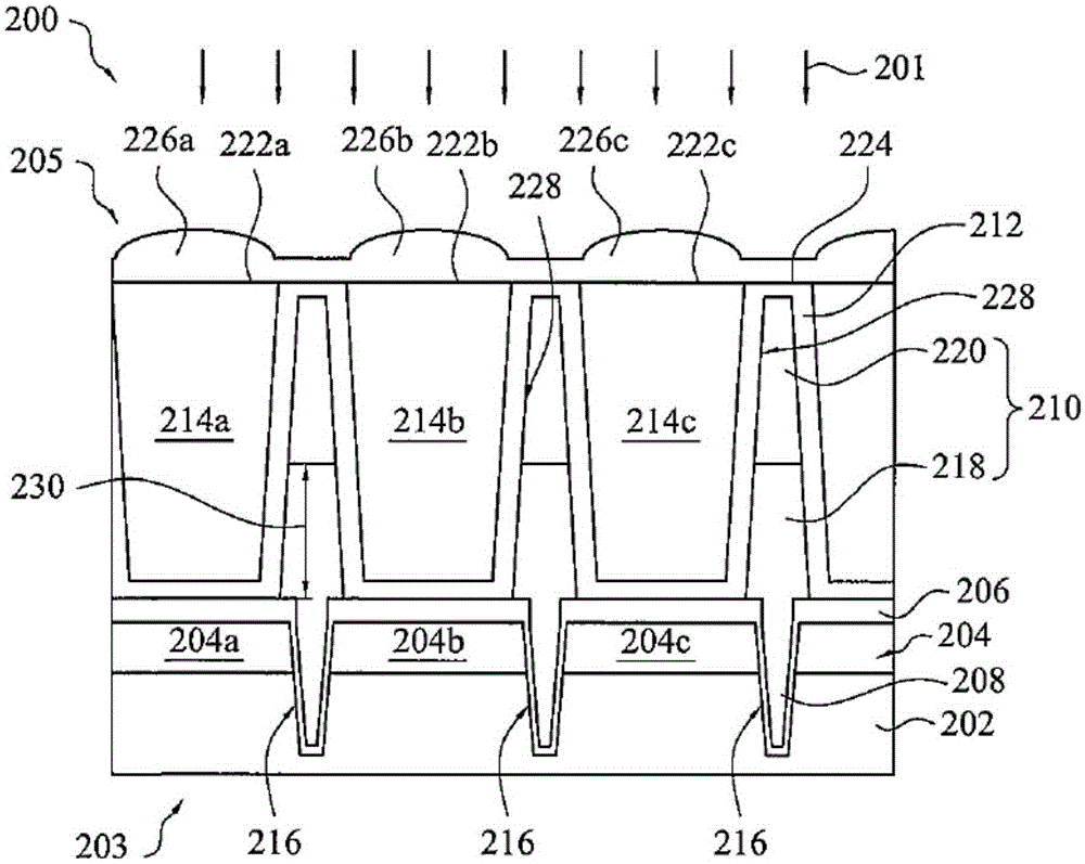
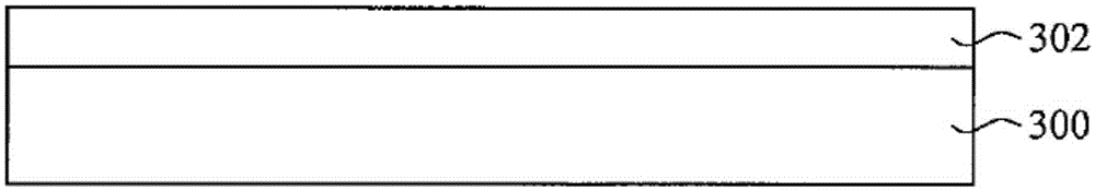
[0015] The following disclosure provides many different embodiments or examples for implementing different features of the presented subject matter. Specific examples of components and arrangements are described below to simplify the present disclosure. Of course, these are only examples and are not intended to limit the invention. For example, in the following description, forming a first part over or on a second part may include embodiments in which the first part and the second part are formed in direct contact, and may also include an embodiment in which the first part and the second part are formed in between. An embodiment where the additional part is such that the first part and the second part are not in direct contact.

[0016] The terminology used herein is for describing particular embodiments only, and shall not be used for limiting the appended claims. For example, the terms "a," "an," or "the" in the singular may also refer to the plural unless otherwise limite...


PUM


Abstract

A semiconductor device includes a substrate, a device layer, an anti-reflective coating layer, reflective structures, a composite grid structure, a passivation layer and color filters. The device layer is disposed on the substrate, in which trenches are formed in the device layer and the substrate. The anti-reflective coating layer conformally covers the device layer, the substrate and the trenches. The reflective structures are disposed on the anti-reflective coating layer in the trenches respectively. The composite grid structure overlies the anti-reflective coating layer and the reflective structures. The composite grid structure includes cavities passing through the composite grid structure, and the composite grid structure includes a metal grid layer and a dielectric grid layer sequentially stacked on the reflective structures. The passivation layer conformally covers the composite grid structure. The color filters respectively fill the cavities. The invention provides the CMOS image sensor structure with the crosstalk improvement.

Description

technical field [0001] The present invention generally relates to the field of semiconductor technology, and more particularly, to a semiconductor device and a manufacturing method thereof. Background technique [0002] Semiconductor image sensors are used to sense light. Generally, semiconductor image sensors include complementary metal-oxide semiconductor (CMOS) image sensors (CIS) and charge-coupled device (CCD) sensors, which are widely used in various applications such as digital still cameras (DSC), mobile phone cameras , Digital Video (DV) and Digital Video Recorder (DVR) applications. These semiconductor image sensors utilize an array of image sensor elements, each including a photodiode and other elements, to absorb light and convert the sensed light into digital data or electrical signals. [0003] Front-illuminated (FSI) CMOS image sensors and back-illuminated (BSI) CMOS image sensors are two types of CMOS image sensors. The FSI CMOS image sensor can be used to...

Claims


Application Information

Patent Timeline
Patent Type & Authority Applications(China)
IPC IPC(8): H01L27/146
CPCH01L27/14625H01L27/1464H01L27/14683H01L27/14621H01L27/14629H01L27/1463H01L27/14689H01L27/14645H01L27/14685
Inventor 郑允玮周俊豪蔡宗翰李国政许永隆
Owner TAIWAN SEMICON MFG CO LTD
Why Eureka
Try Eureka