Alignment compensation system and method for lithographic apparatus

A technology of overlay compensation and photolithography, which is applied in the field of overlay compensation system to achieve the effect of high overlay accuracy

Active Publication Date: 2017-03-29
SHANGHAI MICRO ELECTRONICS EQUIP (GRP) CO LTD
View PDF10 Cites 18 Cited by
  • Summary
  • Abstract
  • Description
  • Claims
  • Application Information

AI Technical Summary

Problems solved by technology

In fact, there are few technologies or solutions aimed at improving the exposure overlay compensation after wafer reorganization

Method used


Image

  • Alignment compensation system and method for lithographic apparatus
  • Alignment compensation system and method for lithographic apparatus
  • Alignment compensation system and method for lithographic apparatus

Examples


Embodiment Construction

[0031] Specific embodiments of the present invention will be described in detail below in conjunction with the accompanying drawings.

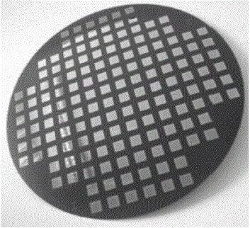
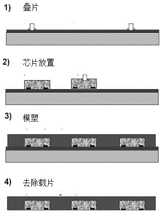
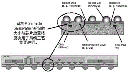
[0032] Figure 4 A lithographic apparatus that can be used to perform the steps of the method of the present invention is schematically shown, comprising: an illuminator 1, an illumination optical system for providing radiation; a mask table 3, for supporting a mask 2; a projection objective 4 , for imaging the pattern onto the reconstituted wafer 5 to be exposed; the workpiece table 6, used for fixing the reconstituted wafer 5 to be exposed; an overlay error measurement and compensation system 7, used for measuring the position 8 and the position of the chip on the reconstituted wafer to be exposed The relative position error of the pattern 9 to be exposed is calculated to obtain a correction model, and the lithography device is controlled to independently drive the mask table 3 drive module, the workpiece table 6 drive module or the objectiv...


PUM


Abstract

The invention discloses an alignment compensation system for a lithographic apparatus. The alignment compensation system comprises an illumination module used for providing a radiation beam, a mask platform used for bearing a pattern, a workbench used for bearing a to-be-exposed reconstituted wafer and supplying motion of at least one degree of freedom, a projection objective used for imaging the pattern to the to-be-exposed reconstituted wafer, and an alignment error measurement and compensation system used for measuring a relative position error between a position of a chip on the to-be-exposed reconstituted wafer and the pattern imaging position, and obtaining a correction model through calculation to compensate the relative position error. Meanwhile, the invention discloses an alignment compensation method for the lithographic apparatus.

Description

technical field [0001] The invention relates to the field of integrated circuit equipment manufacturing, in particular to an overlay compensation system and method for photolithography devices. Background technique [0002] Wafer Level Package (WLP) is based on Ball Grid Array (BGA) technology and is an improved and enhanced Chip size package (CSP). Some people refer to WLP as Wafer Level - Chip Scale Package (WLP-CSP). Wafer-level packaging technology is a technology that performs packaging and testing on the entire wafer and then cuts it to obtain a single finished chip. The size of the packaged chip is exactly the same as that of the bare chip, which conforms to the market's increasingly light, small, short and thin microelectronic products. Requirements for modernization and low price. Fan-out WLP (fan-out WLP) is a type of wafer-level packaging in which the chip is surrounded by adaptive materials scattered on the package area outside the chip. Using wafer-level mold...

Claims


Application Information

Patent Timeline
Patent Type & Authority Applications(China)
IPC IPC(8): G03F7/20
Inventor 陈海华吴凌风任书铭束奇伟韩传有
Owner SHANGHAI MICRO ELECTRONICS EQUIP (GRP) CO LTD
Why Eureka
Try Eureka