Preparation method of polysilicon layer, thin film transistor, array substrate and display device

A polysilicon thin film, polysilicon layer technology, applied in transistors, semiconductor devices, electric solid devices, etc., can solve the problems of poor grain uniformity, inability to effectively control the area, inability to effectively control the grain growth direction, etc., to achieve good performance, Good crystallization effect

Active Publication Date: 2018-04-10
BOE TECH GRP CO LTD
View PDF5 Cites 0 Cited by
  • Summary
  • Abstract
  • Description
  • Claims
  • Application Information

AI Technical Summary

Problems solved by technology

[0005] Although the method of excimer laser annealing is easy to realize large-area polysilicon film formation, there are still shortcomings in the preparation process that cannot effectively control the grain growth direction and poor grain uniformity, and thus cannot effectively control the occurrence of grain boundaries. area

Method used


Image

  • Preparation method of polysilicon layer, thin film transistor, array substrate and display device
  • Preparation method of polysilicon layer, thin film transistor, array substrate and display device
  • Preparation method of polysilicon layer, thin film transistor, array substrate and display device

Examples


preparation example Construction

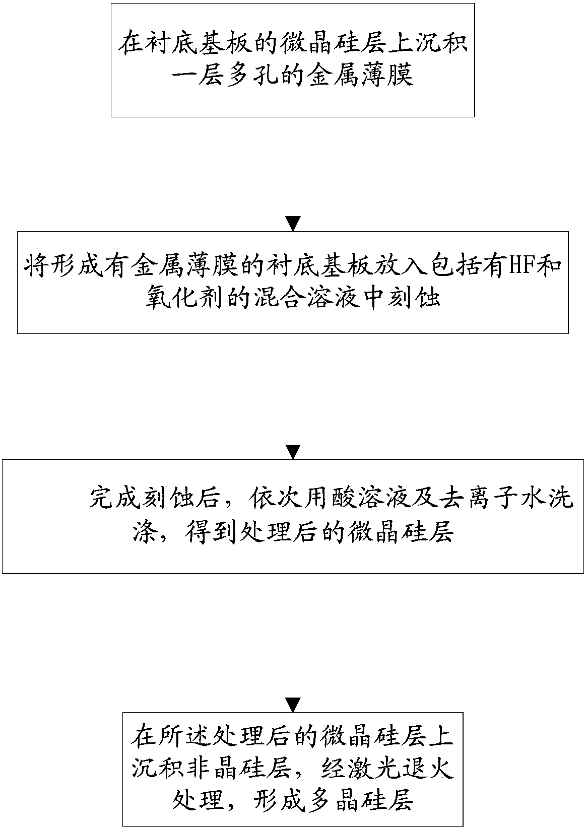
[0035] The embodiment of the present invention discloses a method for preparing a polysilicon layer, comprising the following steps:

[0036] Deposit a layer of porous metal thin film on the microcrystalline silicon layer of the base substrate;

[0037] Etching the base substrate on which the metal thin film is formed in a mixed solution including hydrogen fluoride and an oxidizing agent;

[0038] After the etching is completed, wash with acid solution and deionized water in sequence to obtain the treated microcrystalline silicon layer;

[0039] An amorphous silicon layer is deposited on the treated microcrystalline silicon layer, and a polycrystalline silicon layer is formed through laser annealing treatment.

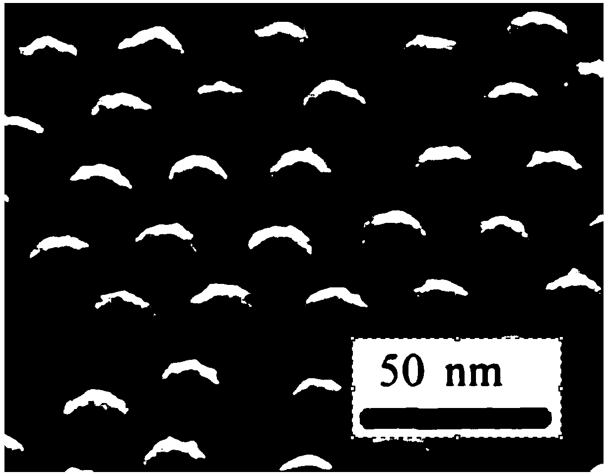
[0040] In the present invention, a porous metal film is deposited on the microcrystalline silicon layer, and the metal film is used to catalyze the etching of the microcrystalline silicon layer. The microcrystalline silicon in the metal-covered area is quickly corrode...

Embodiment 1

[0093] Deposit and form a SiN buffer layer with a thickness of 50-100 nm on the glass substrate.

[0094] A microcrystalline silicon layer with a thickness of 5-10 nm is deposited on the buffer layer.

[0095] The glass substrate after depositing the microcrystalline silicon layer was placed in hydrogen fluoride / AgNO 3 (the concentration of hydrogen fluoride is 3.0-5.0mol / L, the concentration of silver nitrate is 0.01-0.03mol / L) a porous Ag layer is deposited in the solution, and the time is about 60s;

[0096] At a reaction temperature of 50-80°C, the glass substrate is immersed in hydrogen fluoride / Fe(NO 3 ) 3 (the concentration of hydrogen fluoride is 0.2-0.5mol / L, the concentration of ferric nitrate is 8.0-12.0mol / L) and etch for 150-300s;

[0097] Take out the glass substrate, remove the Ag layer with HNO3 (the concentration of nitric acid is 4.0-6.0mol / L), wash it with a large amount of deionized water and then dry it; use PECVD equipment to deposit a 40-50nm amorphou...

Embodiment 2

[0103] Deposit and form a SiO buffer layer with a thickness of 150-300nm on the glass substrate.

[0104] A microcrystalline silicon layer with a thickness of 5-10 nm is deposited on the buffer layer.

[0105] The glass substrate after depositing the microcrystalline silicon layer was placed in hydrogen fluoride / AgNO 3 (the concentration of hydrogen fluoride is 3.0-5.0mol / L, the concentration of silver nitrate is 0.01-0.03mol / L) a porous Ag layer is deposited in the solution, and the time is about 60s;

[0106] At a reaction temperature of 50-80°C, immerse the glass substrate in hydrogen fluoride / H 2 o 2 (the concentration of hydrogen fluoride is 0.2-0.5mol / L, and the concentration of hydrogen peroxide is 0.04-0.08mol / L), etch for 150-300s;

[0107] Remove the glass substrate with HNO 3(The concentration of nitric acid is 4.0-6.0mol / L) to remove the Ag layer, wash it with a large amount of deionized water and dry it; use PECVD equipment to deposit a 40-50nm amorphous silic...


PUM

PropertyMeasurementUnit
thicknessaaaaaaaaaa
thicknessaaaaaaaaaa
thicknessaaaaaaaaaa

Abstract

The invention relates to the display field, and provides a method for preparing a polysilicon layer: depositing a layer of porous metal thin film on the microcrystalline silicon layer of the base substrate; putting the base substrate formed with the metal thin film into the Etching in a mixed solution of an oxidizing agent; after the etching is completed, wash with an acid solution and deionized water in sequence to obtain a treated microcrystalline silicon layer; deposit an amorphous silicon layer on the treated microcrystalline silicon layer, and Laser annealing treatment to form a polysilicon layer. The invention also provides a thin film transistor whose polysilicon layer is prepared by the method. The invention uses the metal thin film as a catalyst to catalyze the etching of the microcrystalline silicon layer, so that silicon seeds with uniform growth direction and uniform size are formed on the surface of the microcrystalline silicon layer. On the basis of the silicon seed crystal, amorphous silicon is deposited and laser annealed to form polycrystalline silicon with a grain size of 350-360nm and 3σ<140nm. The grain growth direction is consistent, and the area where the grain boundary appears is effectively controlled.

Description

technical field [0001] The invention relates to the display field, in particular to a preparation method of a polysilicon layer, a thin film transistor, an array substrate and a display device. Background technique [0002] A thin film transistor is mainly composed of a source, a drain, a gate, an active layer, and a gate insulating layer, among which the active layer and the gate insulating layer are two key layers that determine the performance of a thin film transistor. According to the different materials of the active layer, thin film transistors can be divided into single crystal silicon thin film transistors (c-Si TFT), amorphous silicon thin film transistors (a-Si TFT), polycrystalline silicon thin film transistors (p-SiTFT), organic thin film transistors (OTFT) and zinc oxide thin film transistor (ZnO TFT). [0003] Among them, polysilicon thin film transistors are more suitable for large-capacity high-voltage transistors due to their advantages such as high electr...

Claims


Application Information

Patent Timeline
Patent Type & Authority Patents(China)
IPC IPC(8): H01L21/02H01L29/786H01L27/12
CPCH01L21/02381H01L21/02675H01L27/1222H01L29/786H01L21/02422H01L21/0245H01L21/02488H01L21/02513H01L21/02532H01L21/02658H01L21/02686H01L21/02595H01L29/78675H01L27/1285
Inventor 卜倩倩
Owner BOE TECH GRP CO LTD
Why Eureka
Try Eureka