Room temperature NO2 sensor based on in-situ growth nano In2O3 on surface of non-metal mineral electrode substrate and preparation method

A non-metallic mineral and substrate surface technology, applied in nanotechnology for materials and surface science, nanotechnology for sensing, nanotechnology, etc., can solve the problems of complex preparation methods, slow recovery speed, and singleness , to achieve the effects of simple synthesis process, increased density and reduced production cost

Active Publication Date: 2019-09-20
NORTHEASTERN UNIV
View PDF9 Cites 2 Cited by
  • Summary
  • Abstract
  • Description
  • Claims
  • Application Information

AI Technical Summary

Problems solved by technology

[0005] For the current In 2 o 3 The preparation method of the gas sensor is relatively complex, single deficiency, and low concentration of NO at room temperature 2 The response / recovery speed of the gas is slow and other problems, the present invention provides a kind of in-situ growth nano-In based on the porous ceramic electrode 2 o 3 NO 2 Sensor and its preparation method, and in the recovery stage of the gas sensor, the surface of the gas-sensitive material is irradiated by a UV ultraviolet lamp to achieve a rapid recovery effect

Method used


Image

  • Room temperature NO2 sensor based on in-situ growth nano In2O3 on surface of non-metal mineral electrode substrate and preparation method
  • Room temperature NO2 sensor based on in-situ growth nano In2O3 on surface of non-metal mineral electrode substrate and preparation method
  • Room temperature NO2 sensor based on in-situ growth nano In2O3 on surface of non-metal mineral electrode substrate and preparation method

Examples


Embodiment 1

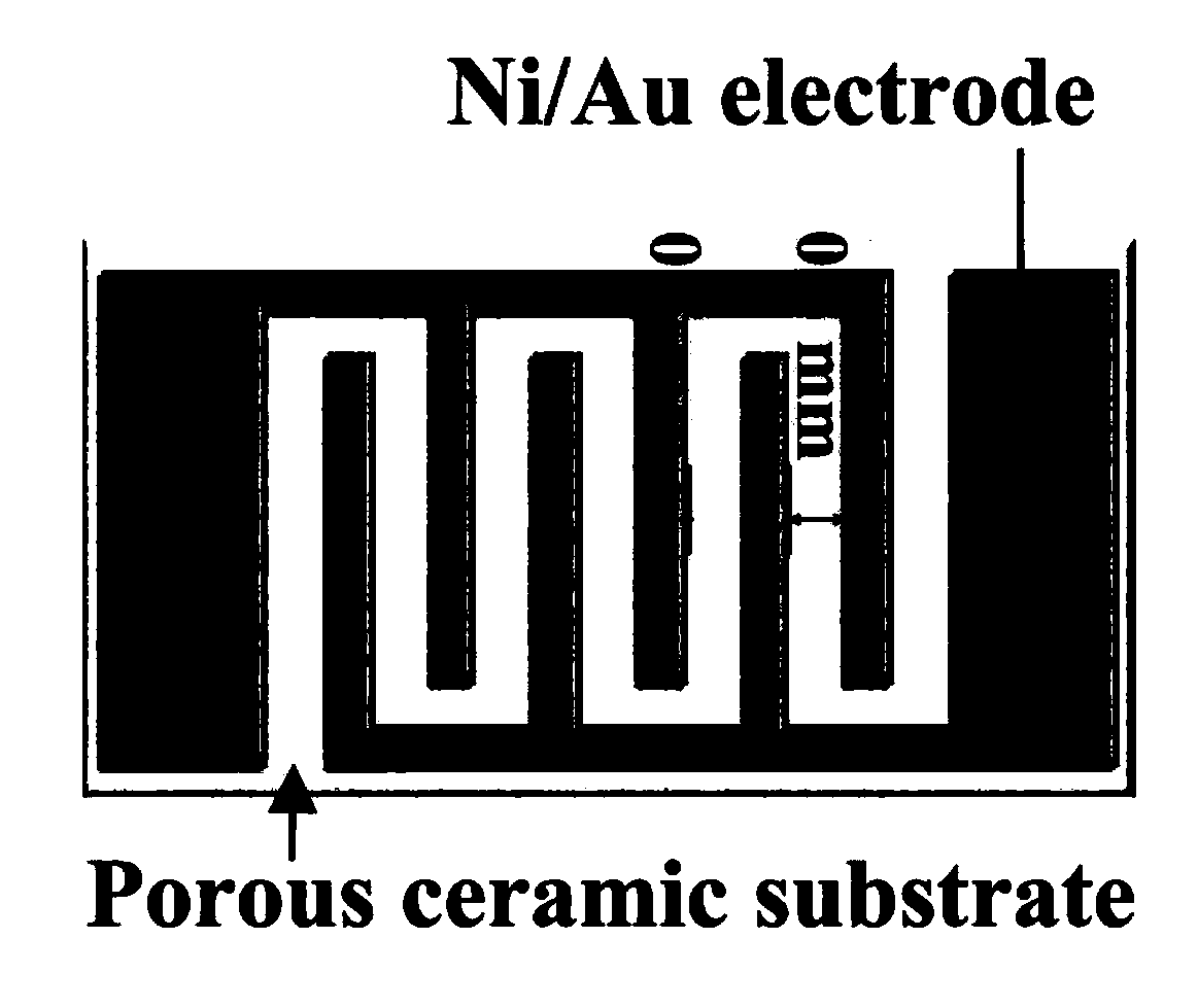
[0030] Based on non-metallic mineral material porous ceramic electrode substrate, its structure schematic diagram is as follows figure 1 shown. The electrodes on the surface of the substrate are formed by sputtering Ni and Au thin films successively on the porous ceramic substrate covered with interdigitated electrode mask by direct current sputtering method, the thickness of the Ni thin film is 10nm, and the thickness of the Au thin film is 50nm, the interdigital width is 0.5mm, and the interdigital spacing is 0.5mm.

[0031] The specific sputtering steps are first sputtering a layer of Ni film, the sputtering current is 17mA, and the sputtering time is 120s; then sputtering a layer of Au film, the sputtering current is 10mA, and the sputtering time is 230s; Sputtering environmental conditions are: argon gas flow rate 200sccm, vacuum degree 90mTorr, sputtering using plasma sputtering apparatus (Hefei Kejing Material Technology Co., Ltd., VTC-16-3HD).

[0032] The material o...

Embodiment 2

[0044] Based on non-metallic mineral material porous ceramic electrode substrate, its structure schematic diagram is as follows figure 1 shown. The electrodes on the surface of the substrate are formed by sputtering Ni and Au thin films successively on the porous ceramic substrate covered with interdigitated electrode mask by direct current sputtering method, the thickness of the Ni thin film is 10nm, and the thickness of the Au thin film 50nm, interdigital width 0.5mm, interdigital spacing 0.5mm.

[0045] The specific sputtering steps are first sputtering a layer of Ni film, the sputtering current is 17mA, and the sputtering time is 120s; then sputtering a layer of Au film, the sputtering current is 10mA, and the sputtering time is 230s; The ambient conditions for sputtering are as follows: argon gas flow rate is 200 sccm, vacuum degree is 90 mTorr, and a plasma sputtering apparatus (Hefei Kejing Material Technology Co., Ltd., VTC-16-3HD) is used for sputtering.

[0046]The...

Embodiment 3

[0057] Based on non-metallic mineral material porous ceramic electrode substrate, its structure schematic diagram is as follows figure 1 shown. The electrodes on the surface of the substrate are formed by sputtering Ni and Au thin films successively on the porous ceramic substrate covered with interdigitated electrode mask by direct current sputtering method, the thickness of the Ni thin film is 10nm, and the thickness of the Au thin film 50nm, interdigital width 0.5mm, interdigital spacing 0.5mm.

[0058] The specific sputtering steps are first sputtering a layer of Ni film, the sputtering current is 17mA, and the sputtering time is 120s; then sputtering a layer of Au film, the sputtering current is 10mA, and the sputtering time is 230s; The ambient conditions for sputtering are: argon flow rate of 200 sccm, vacuum degree of 90 mTorr, and sputtering using a plasma sputtering apparatus (Hefei Kejing Material Technology Co., Ltd., VTC-16-3HD).

[0059] The material of the por...


PUM

PropertyMeasurementUnit
Diameteraaaaaaaaaa
Lengthaaaaaaaaaa
Diameteraaaaaaaaaa

Abstract

The invention discloses a room temperature NO2 sensor based on in-situ growth nano In2O3 on the surface of a non-metal mineral electrode substrate and a preparation method, which belong to the field of gas sensors of metal oxide semiconductor materials. According to the invention, a non-metal mineral porous ceramic electrode is used as a substrate; a direct current sputtering method is used to sputter an interdigital electrode on the surface of the substrate, and the In2O3 nano material hydrothermally grows in situ on the surface thereof; the In2O3 nano material is in a rod-like structure and uniformly and densely distributed on the surface of the substrate, wherein the diameter thereof is 120 to 200nm and the length thereof 0.5 to 1 micron; the rod-like structure is composed of nanoparticles stacked on each other; the nanoparticles are in the structure of In2O3 cubic phase crystals, and the diameter thereof is 10 to 30 nm. The gas sensor can have a fast response and recovery rate for 0.1 to 1 ppm NO2 under room temperature working conditions and under UV light assisted recovery, and has the advantages of excellent selectivity, long-term stability and good application prospects.

Description

technical field [0001] The invention belongs to the technical field of gas sensors of metal oxide semiconductor materials, in particular to a nano-In 2 o 3 Gas sensor and its preparation method, especially related to a kind of in-situ growth nano In on the surface of non-metallic mineral electrode substrate 2 o 3 room temperature NO 2 Sensors and methods of preparation. Background technique [0002] Nitrogen dioxide (NO 2 ) is a toxic and irritating gas emitted from automobile exhaust and industrial production processes, and is one of the main substances that form acid rain and photochemical smog pollution. Even 1ppm of NO 2 It will also cause great harm to the human body, so for low concentrations of NO 2 detection is extremely necessary. Metal oxide semiconductor gas sensors have been widely used in the detection of toxic and harmful gases because of their high sensitivity, online real-time monitoring, miniaturization, easy integration, and strong portability. Curr...

Claims


Application Information

Patent Timeline
IPC IPC(8): G01N27/12B82Y15/00B82Y30/00
CPCB82Y15/00B82Y30/00G01N27/127
Inventor 沈岩柏钟祥熙张津高淑玲魏德洲张云海魏可峰
Owner NORTHEASTERN UNIV
Why Eureka
Try Eureka