A kind of in situ growth nanometer based on the surface of non-metallic mineral electrode substrate 2 o 3 room temperature no 2 Sensor and preparation method
A non-metallic mineral, substrate surface technology, applied in nanotechnology for materials and surface science, nanotechnology for sensing, nanotechnology, etc., can solve the problems of single, slow recovery, complex preparation methods, etc. , to achieve the effect of reducing production cost, increasing density and simple synthesis process
- Summary
- Abstract
- Description
- Claims
- Application Information
AI Technical Summary
Problems solved by technology
Method used
Image
Examples
Embodiment 1
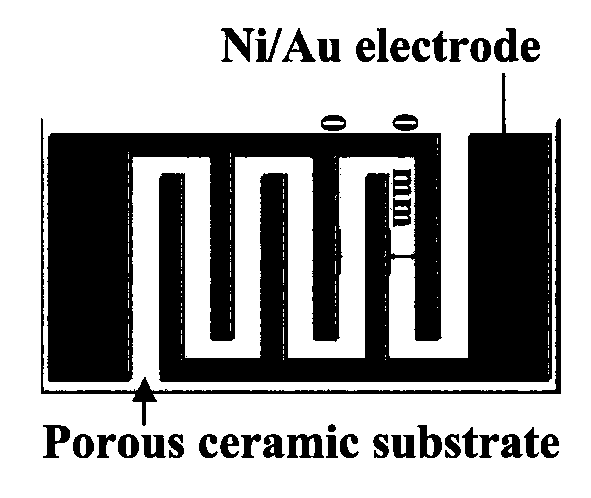
[0030] Based on non-metallic mineral material porous ceramic electrode substrate, its structure schematic diagram is as follows figure 1 shown. The electrodes on the substrate surface are formed by sputtering Ni and Au thin films successively on the porous ceramic substrate covered with interdigitated electrode masks by DC sputtering method, the thickness of the Ni thin film is 10nm, and the thickness of the Au thin film is 50nm, the interdigital width is 0.5mm, and the interdigital spacing is 0.5mm.
[0031] The specific sputtering steps are first sputtering a layer of Ni film, the sputtering current is 17mA, and the sputtering time is 120s; then sputtering a layer of Au film, the sputtering current is 10mA, and the sputtering time is 230s; Sputtering environmental conditions are: argon gas flow rate 200sccm, vacuum degree 90mTorr, sputtering using plasma sputtering apparatus (Hefei Kejing Material Technology Co., Ltd., VTC-16-3HD).
[0032] The material of the porous ceram...
Embodiment 2
[0044] Based on non-metallic mineral material porous ceramic electrode substrate, its structure schematic diagram is as follows figure 1 shown. The electrodes on the substrate surface are formed by sputtering Ni and Au thin films successively on the porous ceramic substrate covered with interdigitated electrode masks by DC sputtering method, the thickness of the Ni thin film is 10nm, and the thickness of the Au thin film 50nm, interdigital width 0.5mm, interdigital spacing 0.5mm.
[0045] The specific sputtering steps are first sputtering a layer of Ni film, the sputtering current is 17mA, and the sputtering time is 120s; then sputtering a layer of Au film, the sputtering current is 10mA, and the sputtering time is 230s; The ambient conditions for sputtering are as follows: argon gas flow rate is 200 sccm, vacuum degree is 90 mTorr, and a plasma sputtering apparatus (Hefei Kejing Material Technology Co., Ltd., VTC-16-3HD) is used for sputtering.
[0046]The material of the p...
Embodiment 3
[0057] Based on non-metallic mineral material porous ceramic electrode substrate, its structure schematic diagram is as follows figure 1 shown. The electrodes on the substrate surface are formed by sputtering Ni and Au thin films successively on the porous ceramic substrate covered with interdigitated electrode masks by DC sputtering method, the thickness of the Ni thin film is 10nm, and the thickness of the Au thin film 50nm, interdigital width 0.5mm, interdigital spacing 0.5mm.
[0058] The specific sputtering steps are first sputtering a layer of Ni film, the sputtering current is 17mA, and the sputtering time is 120s; then sputtering a layer of Au film, the sputtering current is 10mA, and the sputtering time is 230s; The ambient conditions for sputtering are: argon flow rate of 200 sccm, vacuum degree of 90 mTorr, and sputtering using a plasma sputtering apparatus (Hefei Kejing Material Technology Co., Ltd., VTC-16-3HD).
[0059] The material of the porous ceramic electr...
PUM
| Property | Measurement | Unit |
|---|---|---|
| diameter | aaaaa | aaaaa |
| length | aaaaa | aaaaa |
| diameter | aaaaa | aaaaa |
Abstract
Description
Claims
Application Information


