Method for forming conductive layer

A technology of conductive layer and dielectric layer, applied in the field of forming conductive layer, can solve problems such as protrusion of dielectric layer, achieve the effect of small gap, improve product yield, and avoid excessive gap at the junction of grains

Inactive Publication Date: 2019-08-16
SHANGHAI HUAHONG GRACE SEMICON MFG CORP
View PDF4 Cites 0 Cited by
  • Summary
  • Abstract
  • Description
  • Claims
  • Application Information

AI Technical Summary

Problems solved by technology

[0004] The object of the present invention is to provide a method for forming a conductive layer to solve the problem of protrusions on the dielectric layer when etching the conductive layer and a partial thickness of the dielectric layer to form the top circuit layer

Method used


Image

  • Method for forming conductive layer
  • Method for forming conductive layer
  • Method for forming conductive layer

Examples


Embodiment Construction

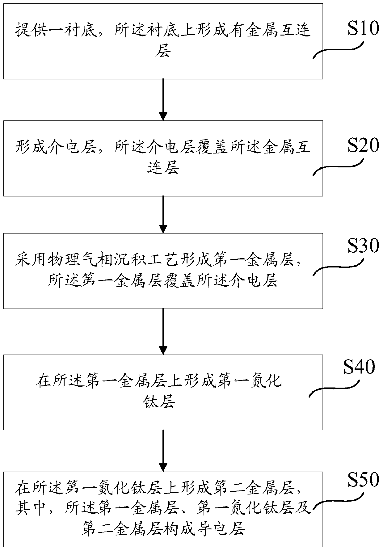
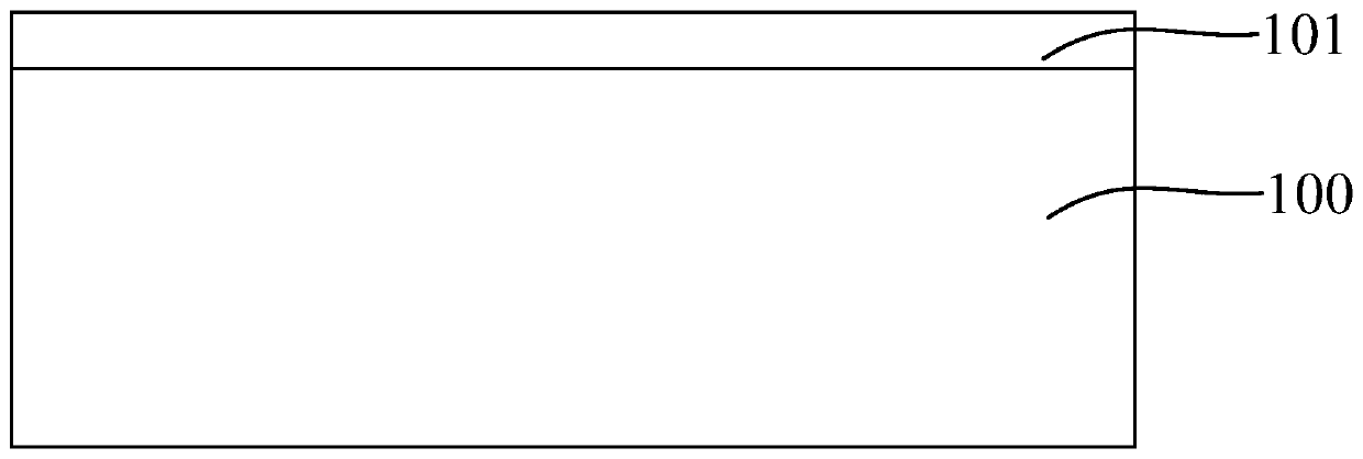
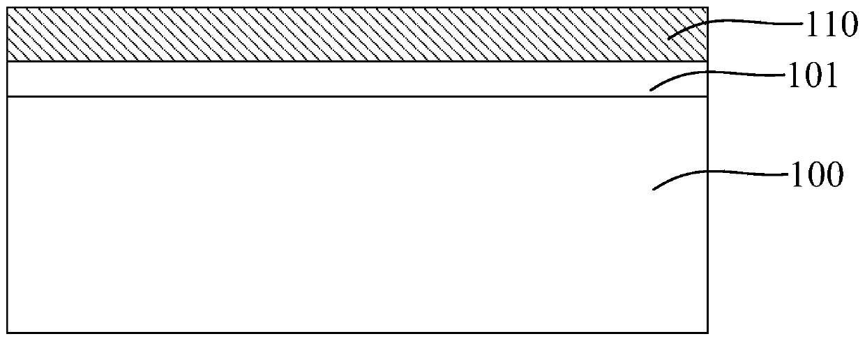
[0026] The method for forming the conductive layer proposed by the present invention will be further described in detail below in conjunction with the accompanying drawings and specific embodiments. Advantages and features of the present invention will be apparent from the following description and claims. It should be noted that all the drawings are in a very simplified form and use imprecise scales, and are only used to facilitate and clearly assist the purpose of illustrating the embodiments of the present invention. In addition, the structures shown in the drawings are often a part of the actual structure. In particular, each drawing needs to display different emphases, and sometimes uses different scales.

[0027] Generally, the conductive layer includes at least a stacked titanium metal layer, a first titanium nitride layer, and an aluminum metal layer. At present, the titanium metal layer is usually formed by a chemical vapor deposition process. The grain growth direct...


PUM

PropertyMeasurementUnit
Surface roughnessaaaaaaaaaa

Abstract

The invention provides a method for forming a conductive layer, comprising the steps of: firstly forming a dielectric layer on a substrate; then forming a first metal layer by a physical vapor deposition process; then forming a first titanium nitride layer on the first metal layer; and finally forming a second metal layer on the first titanium nitride layer, wherein the first metal layer, the first titanium nitride layer, and the second metal layer constitute a conductive layer. The grain growth directions of the first metal layer formed by the physical vapor deposition process tends to be same, so that the grain growth direction of the first titanium nitride layer on the first metal layer and the grain growth directions of respective layers in the second metal layer tend to be the same and a gap at a grain boundary is reduced, thereby reducing the surface roughness of the conductive layer, avoiding a bump defect formed on the dielectric layer when the conductive layer and a portion ofthe thickness of the dielectric layer are subsequently etched, and improving the yield of the products.

Description

technical field [0001] The invention relates to the technical field of semiconductor manufacturing, in particular to a method for forming a conductive layer. Background technique [0002] In a semiconductor device, the conductive layer is generally a titanium metal layer, a first titanium nitride layer and an aluminum metal layer stacked in sequence. The conductive layer is generally deposited on a dielectric layer and used to form a top circuit layer. In order to form the above top circuit layer, technicians need to spin coat a photoresist layer on the conductive layer, perform photoetching on the photoresist layer to form a top circuit pattern on the photoresist layer, and transfer the top circuit pattern to the above the conductive layer to obtain the top circuit layer. [0003] However, currently, after etching the conductive layer and the dielectric layer with a partial thickness to form the top circuit layer, protrusion defects are easily generated on the dielectric l...

Claims


Application Information

Patent Timeline
IPC IPC(8): H01L21/768H01L21/285
CPCH01L21/2855H01L21/76838H01L21/7685
Inventor 刘冲吴继科曹秀亮丁同国
Owner SHANGHAI HUAHONG GRACE SEMICON MFG CORP
Why Eureka
Try Eureka