
High-capacity and metal-insensitive double layer chip-free tag antenna

A tag antenna, chipless technology, applied in antennas, slot antennas, antenna components, etc., can solve the problems of magnetic field line deformation, energy acquisition, and failure to work normally, and achieve the effect of reducing size and improving coding capacity

Active Publication Date: 2017-03-29
SOUTH CHINA UNIV OF TECH
View PDF4 Cites 4 Cited by
  • Summary
  • Abstract
  • Description
  • Claims
  • Application Information

AI Technical Summary

Problems solved by technology

The magnetic field generated by the metal environment interferes with the original magnetic field, causing the magnetic field lines on the metal surface to tend to deform. In the area very close to the metal, it is even parallel to the metal surface. There is no radio frequency field in this area, so it is directly attached to the surface of the metal object. The tag cannot gain energy by cutting the magnetic field line at all and cannot work properly

Method used


Image

  • High-capacity and metal-insensitive double layer chip-free tag antenna
  • High-capacity and metal-insensitive double layer chip-free tag antenna
  • High-capacity and metal-insensitive double layer chip-free tag antenna

Examples


Embodiment

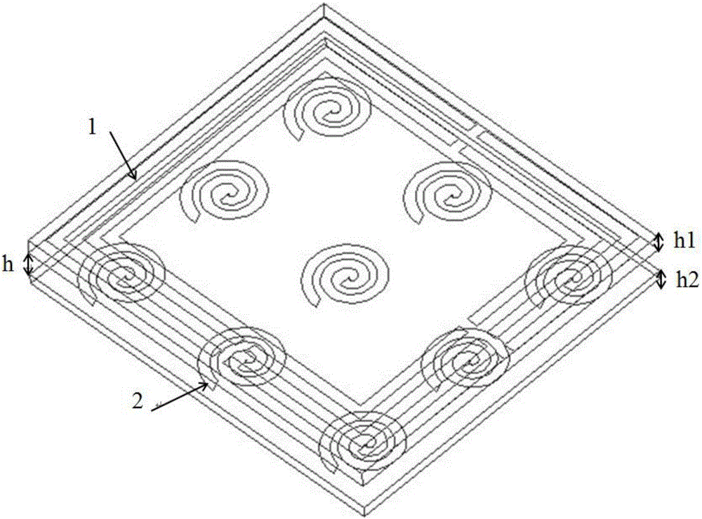
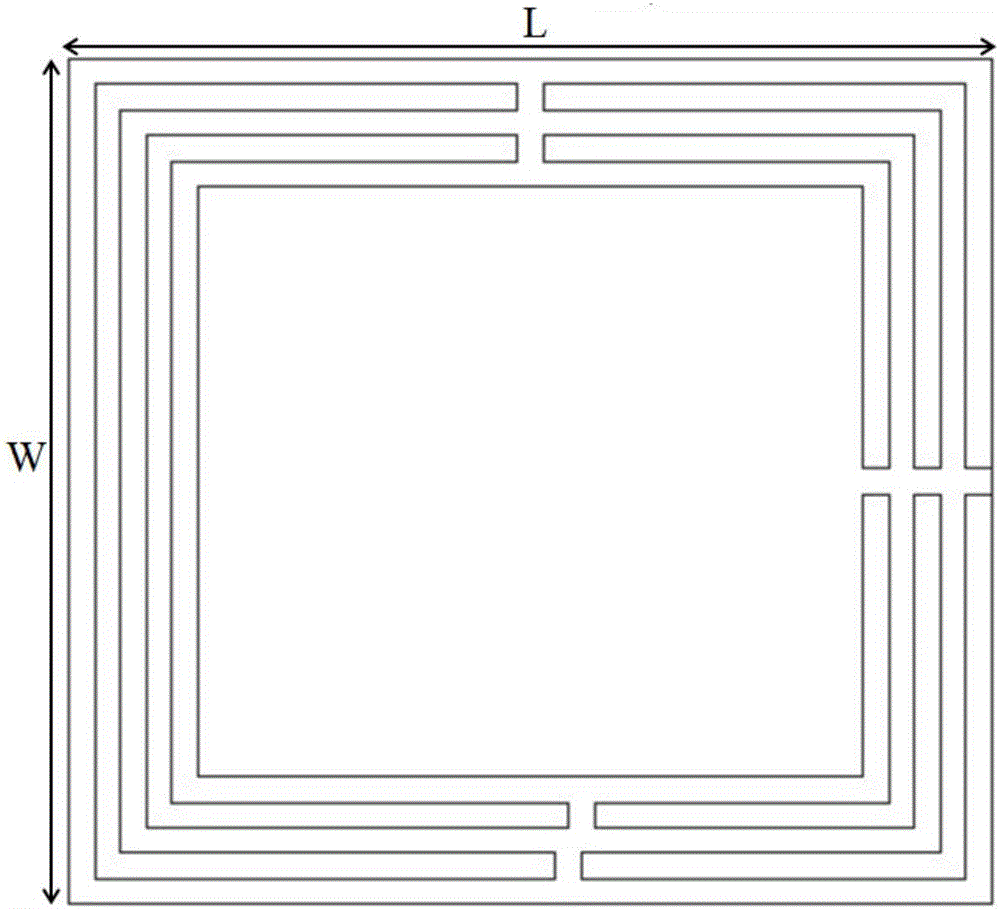
[0029] This embodiment discloses a high-capacity and metal-insensitive double-layer chipless tag antenna, which is used in a radio frequency identification system chipless tag antenna, including an upper dielectric substrate, a lower dielectric substrate, a split ring resonator and a spiral resonator . The split ring resonator and the spiral resonator are printed on the upper dielectric substrate and the lower dielectric substrate respectively, and the split ring resonator and the spiral resonator have different heights in the same vertical plane distributed.

[0030] In a specific embodiment, the split ring resonator is located on the upper surface of the upper dielectric substrate, the spiral resonator is located on the lower surface of the lower dielectric substrate, and the gap between the upper dielectric substrate and the lower dielectric substrate is Air spaced at a height of 0.5mm. The tag antenna disclosed in the present invention utilizes a double-layer structure i...


PUM

PropertyMeasurementUnit
Widthaaaaaaaaaa
Thicknessaaaaaaaaaa
Thicknessaaaaaaaaaa

Abstract

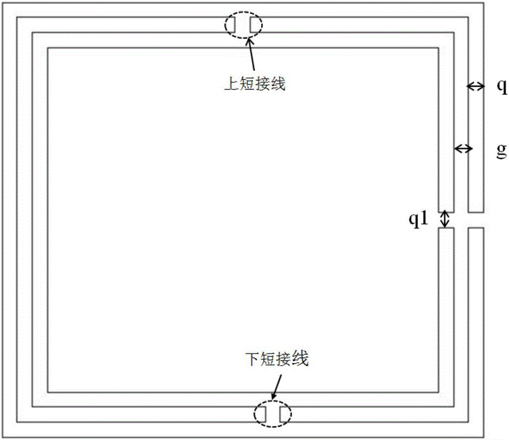
The invention discloses a high-capacity and metal-insensitive double layer chip-free tag antenna, which is used for coding articles in a chip-free tag system. The high-capacity and metal-insensitive double layer chip-free tag antenna comprises two layers of dielectric substrates, a split ring resonator and a spiral resonator, wherein the split ring resonator consists of three coaxial rectangular split rings, and each two adjacent split rings are connected to each other through a pair of upper and lower short connection lines; the spiral resonator consists of nine spiral bodies with the same size; each spiral body is made of copper strips through staggered screwing from inside to outside; and the split ring resonator and the spiral resonator are distributed at different heights in the same vertical plane. The tag antenna disclosed by the invention is a magnetic antenna, and is insensitive to different dielectric substrates to which the antenna is adhered. The tag antenna achieves the metal-insensitive characteristics by using a double layer structure that uses the intermediate layer to separate the air. Meanwhile, as three resonant frequency points can be increased when one unit structure is increased, the tag antenna disclosed by the invention can achieve very high coding capacity.

Description

technical field [0001] The invention relates to the field of chipless tag antennas, in particular to a high-capacity and metal-insensitive double-layer chipless tag antenna. Background technique [0002] Compared with labels such as barcodes, chipless labels have the advantages of low cost, strong practicability, and rapid identification by readers in terms of commodity classification, tracking, and identification. Therefore, they have the potential value of replacing barcodes and being widely used. By encoding different signals '0' or '1', and using different combinations to represent different information, the information of the coded commodity is recorded. However, most tag antennas will add a structural unit for every additional bit of code, so the size of the antenna is increased to a large extent, which is not conducive to the miniaturization of the antenna. [0003] At the same time, in some engineering applications, in order to identify metal goods, labels need to b...

Claims


Application Information

Patent Timeline
IPC IPC(8): H01Q1/22H01Q1/38H01Q13/10
CPCH01Q1/2225H01Q1/38H01Q13/10Y02D30/70
Inventor 黄惠芬苏丽
Owner SOUTH CHINA UNIV OF TECH
Learn More