Epitaxial wafer of light-emitting diode and manufacturing method thereof
A technology of light-emitting diodes and epitaxial wafers, which is applied to electrical components, circuits, semiconductor devices, etc., can solve the problems affecting the luminous brightness and service life of LEDs, and achieve the effect of improving luminous brightness and improving the efficiency of recombination.
- Summary
- Abstract
- Description
- Claims
- Application Information
AI Technical Summary
Problems solved by technology
Method used
Image

Examples
Embodiment 1
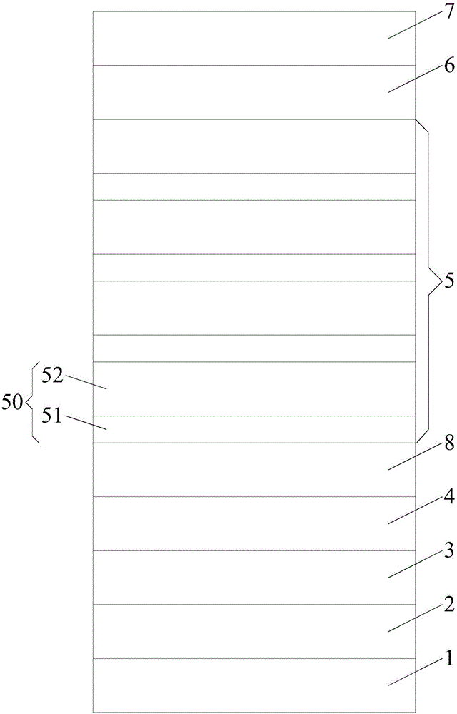
[0026] An embodiment of the present invention provides a light emitting diode epitaxial wafer, see figure 1 The light emitting diode epitaxial wafer includes a substrate 1, and a low-temperature buffer layer 2, an undoped GaN layer 3, an N-type GaN layer 4, a multi-quantum well layer 5, and a P-type electron blocking layer 6 stacked on the substrate 1 in sequence. , P-type GaN layer 7, multi-quantum well layer 5 includes several sublayers 50, sublayer 50 includes quantum well layer 51 and quantum barrier layer 52 stacked on quantum well layer 51, quantum well layer 51 is InGaN layer, quantum barrier Layer 52 is Al x In y GaN layer, 0b GaN, 0<b<0.2 and b<x.
[0027] In an implementation of this embodiment, the quantum barrier layer 52 can be a single layer of Al x In y GaN layer, all monolayer Al x In y The content of the Al component in the GaN layer can be reduced layer by layer along the stacking direction of the light emitting diode epitaxial wafer. For example, alon...
Embodiment 2
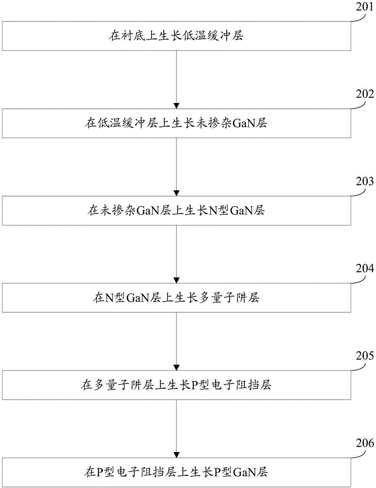
[0039] An embodiment of the present invention provides a method for manufacturing a light-emitting diode epitaxial wafer, see figure 2 , the method flow includes:
[0040] Step 201: growing a low temperature buffer layer on the substrate.
[0041] Step 202: growing an undoped GaN layer on the low-temperature buffer layer.
[0042] Step 203: growing an N-type GaN layer on the undoped GaN layer.
[0043] Step 204: growing a multi-quantum well layer on the N-type GaN layer.
[0044] In this embodiment, the multi-quantum well layer includes several sublayers, the sublayers include a quantum well layer and a quantum barrier layer stacked on the quantum well layer, the quantum well layer is an InGaN layer, and the quantum barrier layer is an Al layer. x In y GaN layer, 0<x<0.5, 0<y<0.5.
[0045] It should be noted that after the growth of the quantum well layer is completed, the In source and the Al source will continue to be supplied to adjust the pressure, temperature, NH 3...
PUM
| Property | Measurement | Unit |
|---|---|---|
| Thickness | aaaaa | aaaaa |
| Thickness | aaaaa | aaaaa |
Abstract
Description
Claims
Application Information
 - R&D
- Intellectual Property
- Life Sciences
- Materials
- Tech Scout
- Unparalleled Data Quality
- Higher Quality Content
- 60% Fewer Hallucinations
Browse by: Latest US Patents, China's latest patents, Technical Efficacy Thesaurus, Application Domain, Technology Topic, Popular Technical Reports.
© 2025 PatSnap. All rights reserved.Legal|Privacy policy|Modern Slavery Act Transparency Statement|Sitemap|About US| Contact US: help@patsnap.com