Semiconductor light emitting device

a technology of semiconductor devices and light emitting devices, which is applied in the direction of semiconductor devices, lasers, semiconductor lasers, etc., can solve the problems of reducing reliability, increasing operating voltage, and increasing operating temperature and operating curren

Inactive Publication Date: 2011-11-10
PANASONIC CORP
View PDF8 Cites 22 Cited by
  • Summary
  • Abstract
  • Description
  • Claims
  • Application Information

AI Technical Summary

Benefits of technology

[0017]The AlGaN layer formed on the active layer can reduce the overflow of the electrons, but forms a potential barrier (ΔEv) in a valence band to holes injected from the p-side electrode to the active layer. Thus, the AlGaN layer functions as an energy barrier.
[0018]In the first and second conventional examples, the overflow of the electrons can be reduced. However, the operating voltage is increased because the energy barrier to the holes is formed.

Problems solved by technology

However, the operating voltage is increased because the energy barrier to the holes is formed.
In the blue-violet nitride semiconductor laser, the increase in operating voltage leads to increase in operating temperature and operating current of the semiconductor laser, thereby reducing reliability, and ranges of temperature and laser output in which stable operation is allowed.

Method used


Image

  • Semiconductor light emitting device
  • Semiconductor light emitting device
  • Semiconductor light emitting device

Examples


first example embodiment

[0058]A semiconductor light emitting device of the first example embodiment will be described below with reference to FIG. 1.

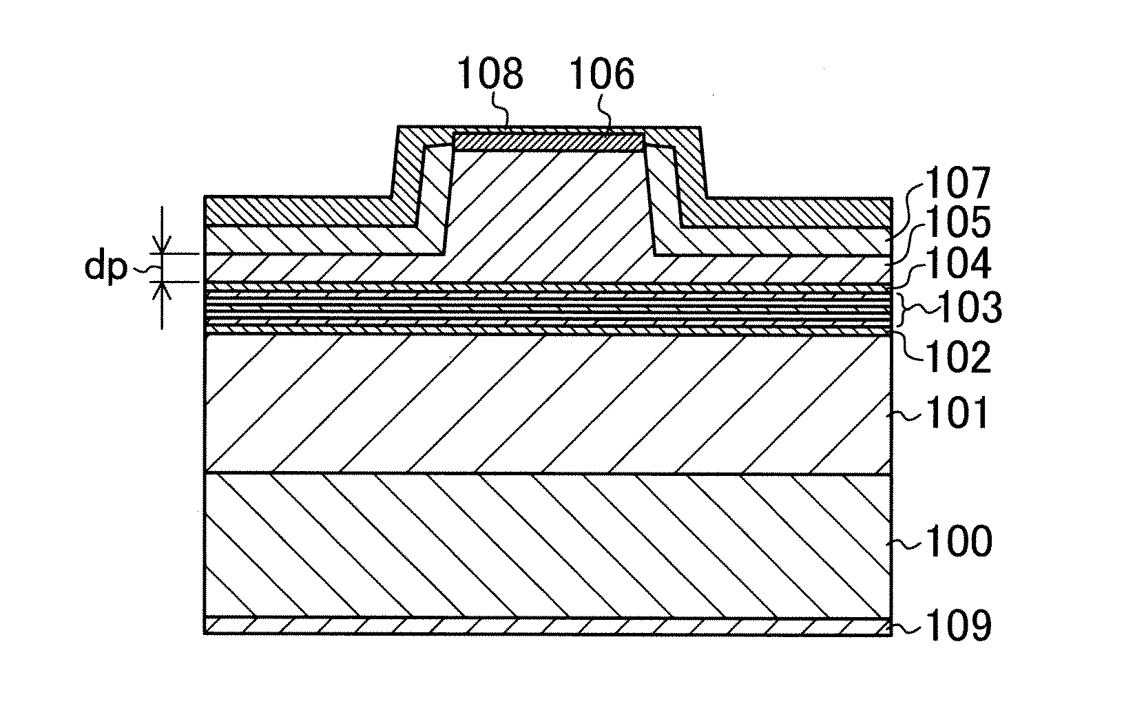
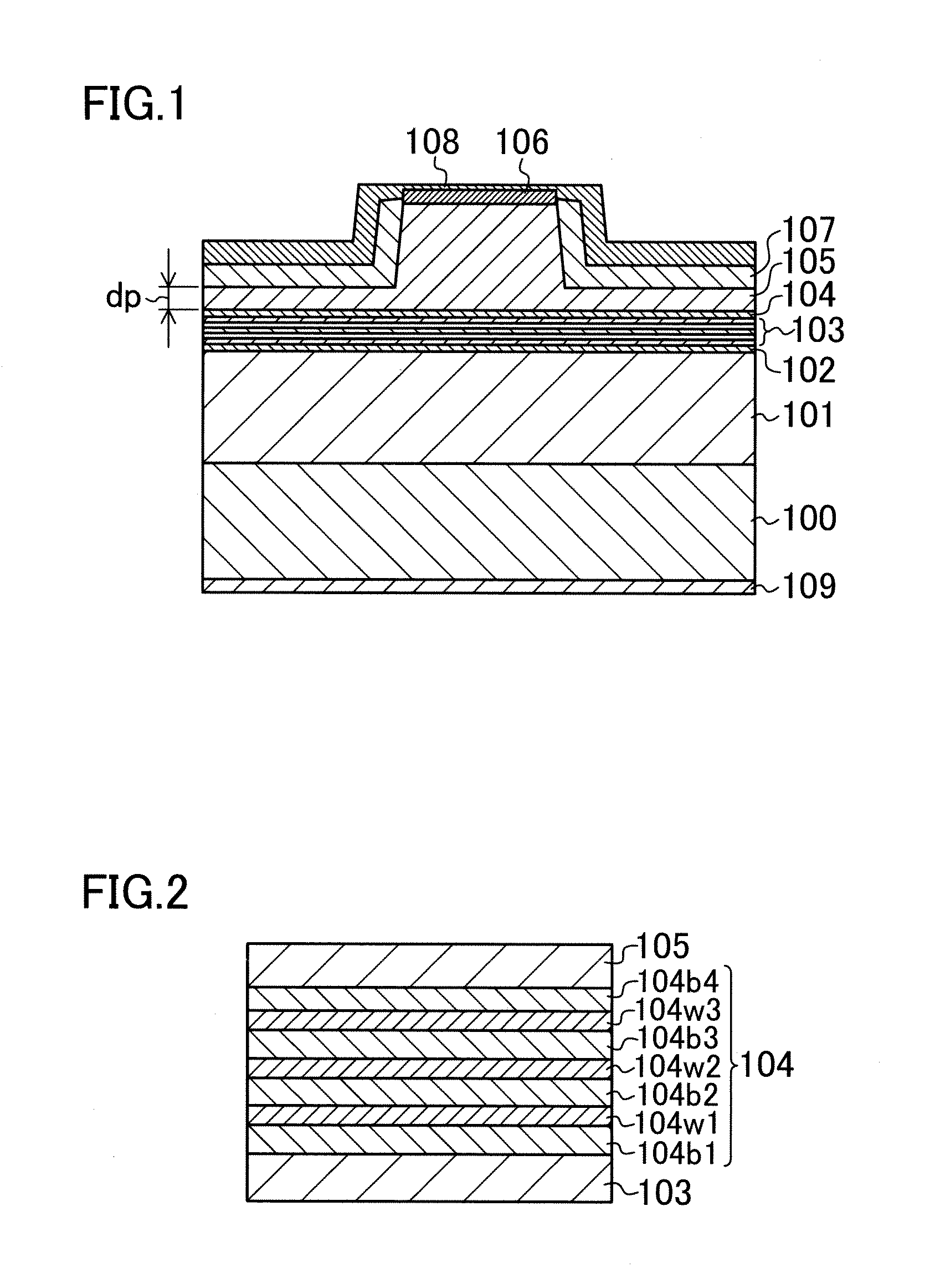
[0059]As shown in FIG. 1, for example, a 2.5 μm thick first cladding layer 101 made of n-type aluminum gallium nitride (AlGaN), and a 86 nm thick guiding layer 102 made of n-type AlGaN are sequentially formed on a gallium nitride (GaN) semiconductor substrate 100. An active layer 103 which includes a multiple quantum well structure, and is made of indium gallium nitride (InGaN)-based material, for example, is formed on the guiding layer 102, and a p-type quantum well electron barrier layer 104 is formed on the active layer 103. A second cladding layer 105 which is made of p-type AlGaN, and has a ridge is formed on the quantum well electron barrier layer104, and a 0.1 μm thick contact layer 106 made of p-type GaN is formed on a top surface of the ridge of the second cladding layer 105. A dielectric current block layer 107 which is made of SiN, and is transparen...

second example embodiment

[0085]A semiconductor light emitting device of a second example embodiment will be described below. In the second example embodiment, the same components as those described in the first example embodiment will not be described in detail, and only the difference between the second and first example embodiments will be described below.

[0086]In the second example embodiment, AlGaN layers having the Al composition ratio of 0.3 are used as the electron trapping barrier layers. The third well layer 104w3, the second well layer 104w2, and the first well layer 104w1 are made of AlGaN having different Al composition ratios of 0.05, 0.15, and 0.25, respectively. Different from the first example embodiment, the first well layer 104w1, the second well layer 104w2, and the third well layer 104w3 have thicknesses of 2 nm, 4 nm, and 6 nm, respectively.

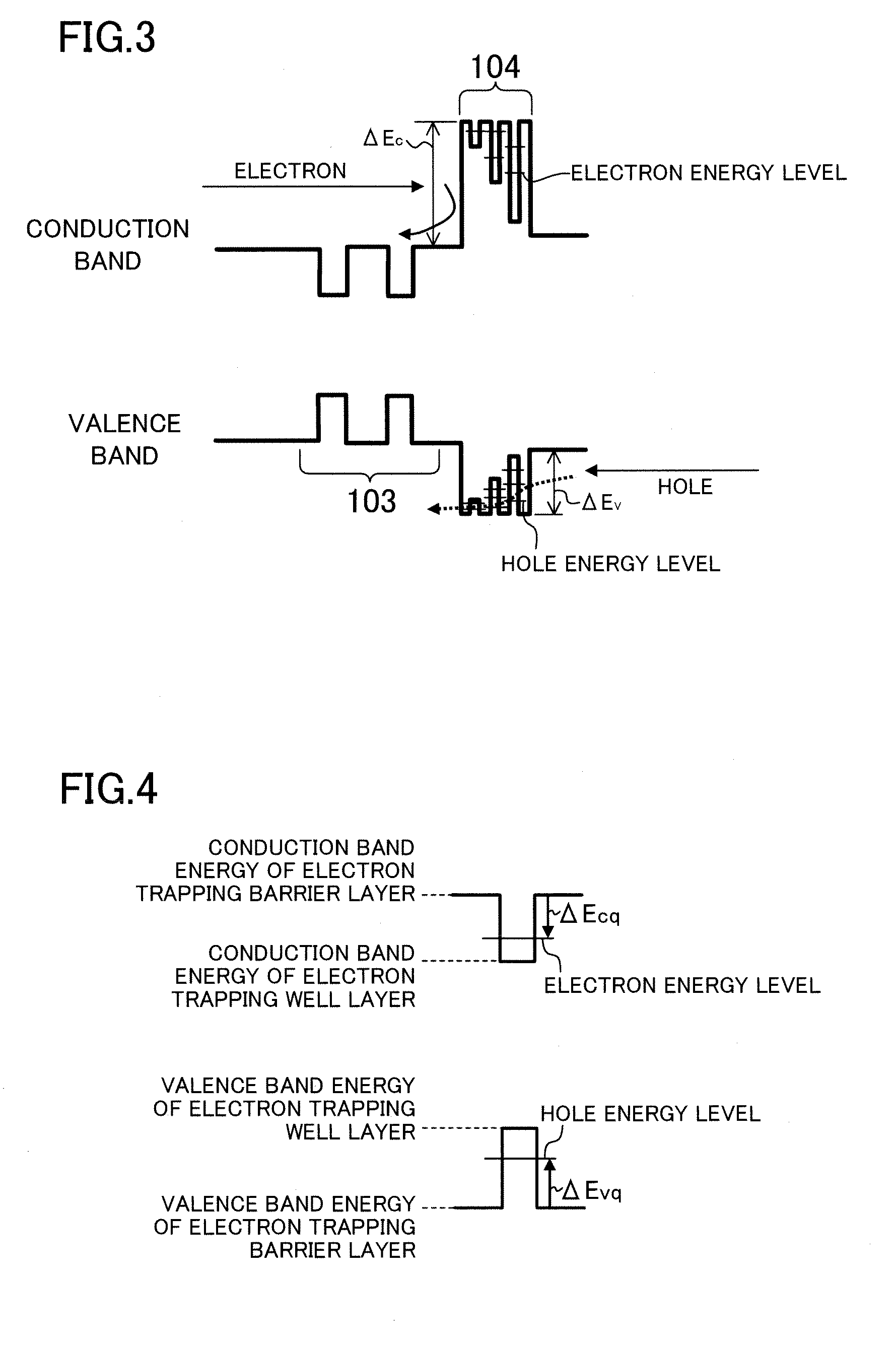
[0087]Quantum levels of electrons and holes formed in each of the electron trapping well layers of the second example embodiment will be described b...

third example embodiment

[0092]A semiconductor light emitting device of a third example embodiment will be described below. In the third example embodiment, the same components as those of the first example embodiment will not be described in detail, and only the difference between the third and first example embodiments will be described below.

[0093]In the third example embodiment, AlGaN layers having the Al composition ratio of 0.3 are used as the electron trapping barrier layers, and 4 nm thick aluminum gallium indium nitride (AlGaInN) layers are used as the electron trapping well layers. The Al composition ratios of the third well layer 104w3, the second well layer 104w2, and the first well layer 104w1 are 0.05, 0.15, and 0.25, respectively.

[0094]The electron trapping barrier layers experience tensile strain due to the difference in lattice constant between the electron trapping barrier layers and the semiconductor substrate 100. When the Al composition ratio in the electron trapping barrier layers is i...


PUM


Abstract

A semiconductor light emitting device includes: a first cladding layer made of a first conductivity type group III nitride semiconductor; an active layer formed on the first cladding layer; a quantum well electron barrier layer which is formed on the active layer, and includes electron trapping barrier layers made of AlxbGaybIn1-xb-ybN (0≦xb<1, 0<yb≦1, 0≦1-xb-yb<1), and two or more electron trapping well layers made of AlxwGaywIn1-xw-ywN (0≦xw<1, 0<yw≦1, 0≦1-xw-yw<1); and a second cladding layer which is formed on the quantum well electron barrier layer, and is made of a second conductive type group III nitride semiconductor. Each of the electron trapping well layers is formed between the electron trapping barrier layers, and band gap energies of the electron trapping well layers increase with decreasing distance from the active layer.

Description

CROSS-REFERENCE TO RELATED APPLICATION[0001]This application claims priority to Japanese Patent Application No. 2010-107181 filed on May 7, 2010, the disclosure of which including the specification, the drawings, and the claims is hereby incorporated by reference in its entirety.BACKGROUND[0002]The present disclosure relates to semiconductor light emitting devices, particularly to high-power semiconductor light emitting devices.[0003]Due to increase in capacity of optical disc systems in recent years, Blu-ray (registered trademark) optical disc systems having larger storage capacity than compact discs (CD) and digital versatile discs (DVD) have appeared on the market. Semiconductor laser devices which use a nitride compound, and are capable of producing blue-violet laser light having a wavelength of 405 nm (hereinafter referred to as semiconductor lasers) have been and are being practically used.[0004]The semiconductor lasers used as light sources of the optical disc systems are req...

Claims


Application Information

Patent Timeline
Patent Type & Authority Applications(United States)
IPC IPC(8): H01L33/06
CPCB82Y20/00H01L33/04H01L33/145H01L33/20H01S5/34333H01S5/22H01S5/3211H01S5/3407H01S5/2009
Inventor TAKAYAMA, TORU
Owner PANASONIC CORP
Why Eureka
Try Eureka