A kind of semiconductor device and its preparation method, electronic device

An electronic device and semiconductor technology, which is applied in semiconductor devices, semiconductor/solid-state device manufacturing, electric solid-state devices, etc., can solve problems affecting SRAM performance, fin damage, easy loss, etc.

Active Publication Date: 2019-10-25
SEMICON MFG INT (SHANGHAI) CORP +1
View PDF3 Cites 0 Cited by
  • Summary
  • Abstract
  • Description
  • Claims
  • Application Information

AI Technical Summary

Problems solved by technology

[0005] First of all, the first one is to perform channel stop ion implantation after fin formation, the main problem is damage to fins, especially for NMOS, where NMOS punch-through is more serious than PMOS, mainly because NMOS punch-through is done with B or BF 2 , while PMOS uses AS; B ions are relatively easy to lose (LOSS)
[0006] Another process is to perform channel stop ion implantation before fin formation, which also affects the performance of SRAM due to the impact of lateral diffusion

Method used


Image

  • A kind of semiconductor device and its preparation method, electronic device
  • A kind of semiconductor device and its preparation method, electronic device
  • A kind of semiconductor device and its preparation method, electronic device

Examples


Embodiment 1

[0038] The semiconductor device and the preparation method of the present invention will be further described below in conjunction with the accompanying drawings, wherein, Figures 1a-1h It is a schematic diagram of the preparation process of the semiconductor device described in the present invention; figure 2 It is a process flow chart for preparing the semiconductor device of the present invention.

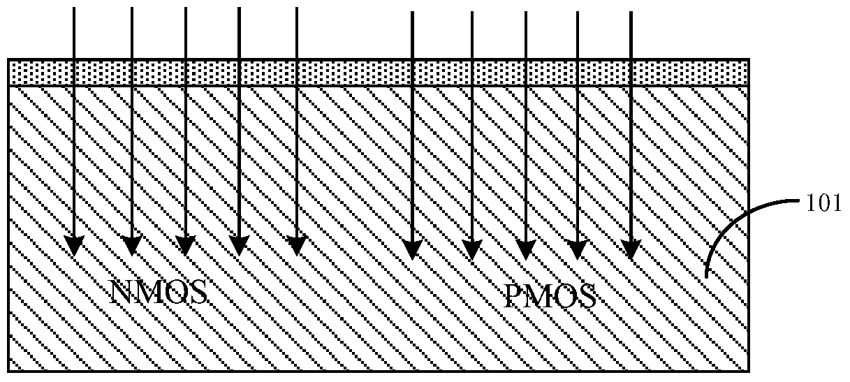
[0039] Step 101 is executed to provide a semiconductor substrate 101 and perform ion implantation to form a well.

[0040] In this step, the semiconductor substrate 101 may be at least one of the materials mentioned below: silicon, silicon-on-insulator (SOI), silicon-on-insulator (SSOI), silicon-germanium-on-insulator (S- SiGeOI), silicon germanium on insulator (SiGeOI) and germanium on insulator (GeOI), etc.

[0041] Wherein the semiconductor substrate 101 includes an NMOS region and a PMOS region, so as to form NMOS devices and PMOS devices in subsequent steps.

[0042] Ne...

Embodiment 2

[0080] The present invention also provides a semiconductor device, and the present invention also provides a semiconductor device, and the semiconductor device is prepared by the method described in Embodiment 1.

[0081] The semiconductor device includes:

[0082] semiconductor substrate 101;

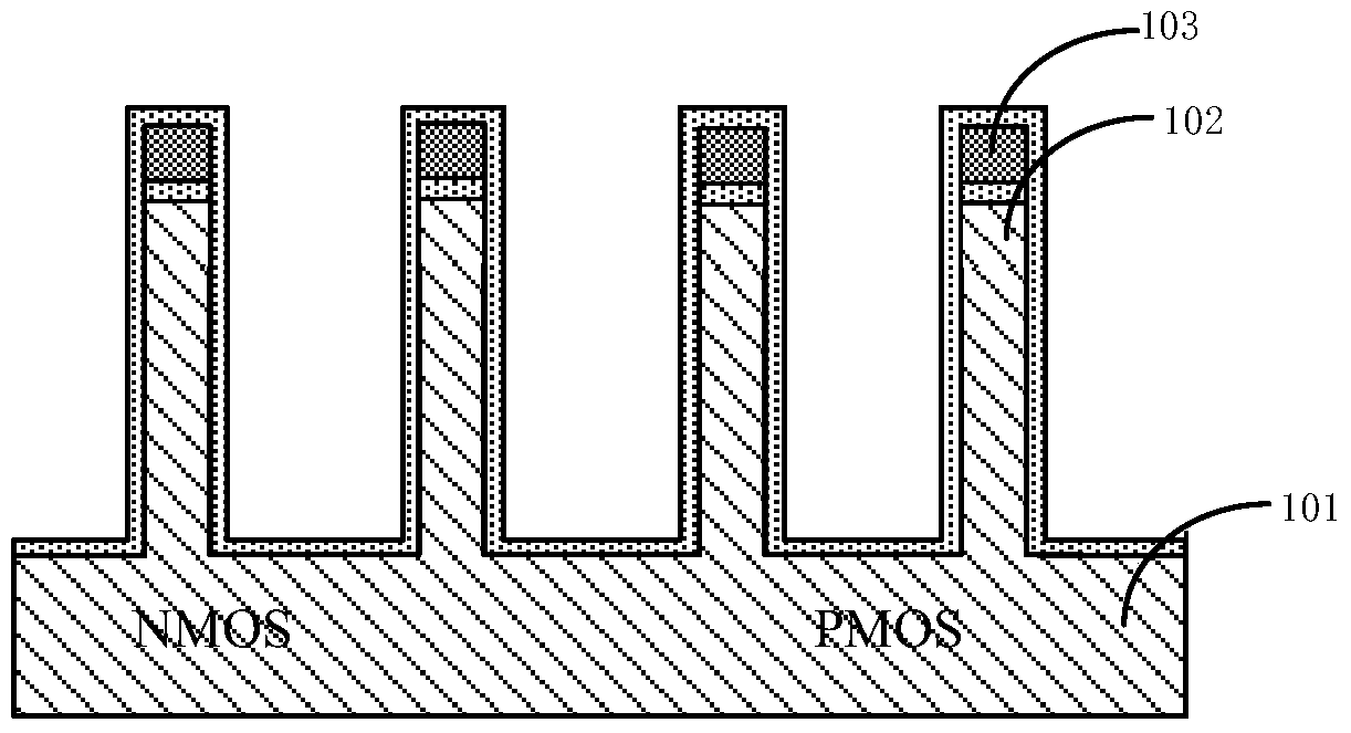
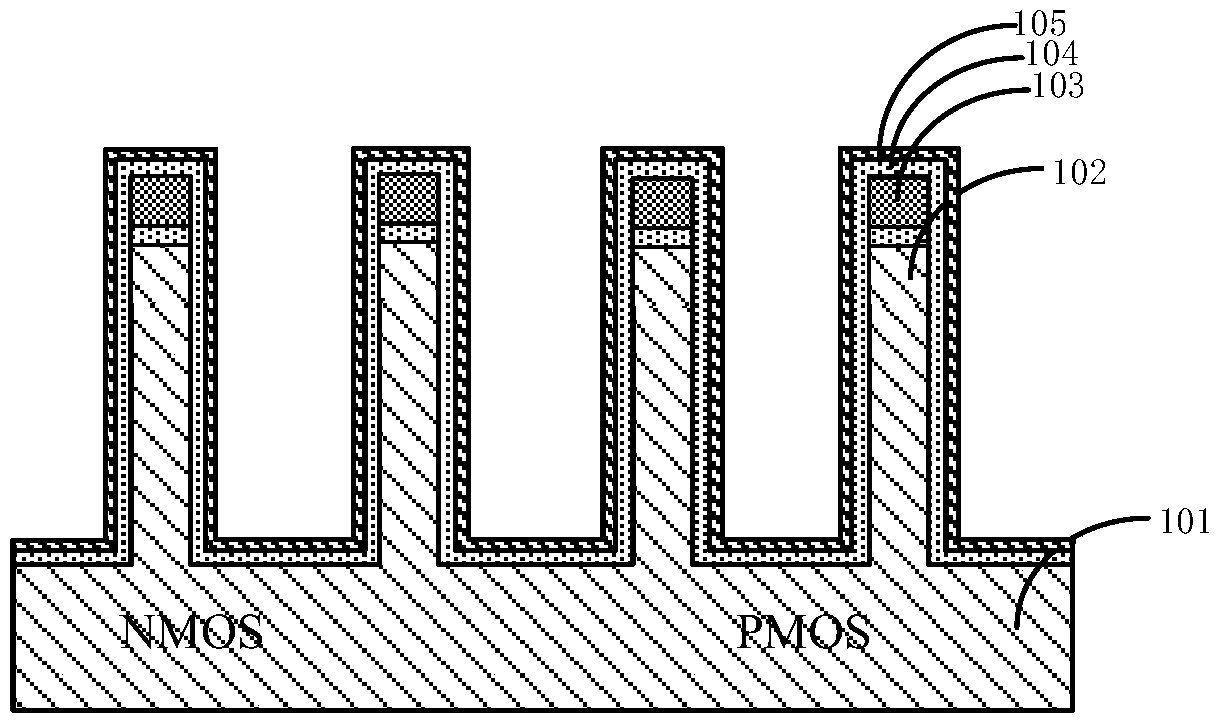
[0083] a plurality of fin structures 102 located in the semiconductor substrate;

[0084] a channel stop implant layer located in the channel region of the fin structure in the semiconductor substrate;

[0085] A diffusion stop layer is located above the channel stop injection layer in the fin structure.

[0086] Wherein, the semiconductor substrate 101 may be at least one of the materials mentioned below: silicon, silicon-on-insulator (SOI), silicon-on-insulator (SSOI), silicon-germanium-on-insulator (S-SiGeOI ), silicon germanium on insulator (SiGeOI) and germanium on insulator (GeOI), etc.

[0087] Wherein the semiconductor substrate 101 includes an NMOS region and a PMOS region...

Embodiment 3

[0094] The present invention also provides an electronic device, including the semiconductor device described in the second embodiment. Wherein, the semiconductor device is the semiconductor device described in the second embodiment, or the semiconductor device obtained according to the preparation method described in the first embodiment.

[0095] The electronic device of this embodiment can be any electronic product or equipment such as mobile phone, tablet computer, notebook computer, netbook, game console, TV set, VCD, DVD, navigator, camera, video recorder, voice recorder, MP3, MP4, PSP, etc. , can also be any intermediate product including the semiconductor device. The electronic device according to the embodiment of the present invention has better performance due to the use of the above-mentioned semiconductor device.


PUM


Abstract

The invention relates to a semiconductor device, a preparation method therefor, and an electronic device. The method comprises the steps: S1, providing a semiconductor substrate, and carrying out the trench immobile ion implantation of the semiconductor substrate; S2, patterning the semiconductor substrate, so as to form a plurality of fins at intervals; S3, forming a protection layer on the fins; S4, depositing an isolation material layer so as to cover the fins, carrying out the back etching of the isolation material layer so as to expose a part of fins and form the fins with the target height; S5, executing diffusion immobile ion implantation in the isolation material layer, so as to prevent the diffusion of trench immobile ions. A device prepared through the method can improve mismatching performances, caused by the lateral diffusion and implantation of NMOS trench immobile ions, of an SRAM device. Through the improvement of the method provided by the invention, the performance and yield of the semiconductor device is further improved.

Description

technical field [0001] The present invention relates to the field of semiconductors, in particular, the present invention relates to a semiconductor device, a preparation method thereof, and an electronic device. Background technique [0002] With the continuous development of semiconductor technology, the improvement of integrated circuit performance is mainly achieved by continuously shrinking the size of integrated circuit devices to increase its speed. At present, due to the demand for high device density, high performance, and low cost, the semiconductor industry has advanced to the nanotechnology process node, and the fabrication of semiconductor devices is limited by various physical limits. [0003] As the size of CMOS devices continues to shrink, the short-channel effect has become a key factor affecting device performance. Compared with existing planar transistors, FinFETs are advanced semiconductor devices used for 20nm and below process nodes, which can effective...

Claims


Application Information

Patent Timeline
Patent Type & Authority Patents(China)
IPC IPC(8): H01L21/8238H01L27/092
CPCH01L21/823807H01L21/823821H01L21/823878H01L27/0924H01L29/66803
Inventor 周飞
Owner SEMICON MFG INT (SHANGHAI) CORP
Why Eureka
Try Eureka