Copper foil substrate manufacturing method

A technology for a copper foil substrate and a manufacturing method, which is applied in the manufacture of printed circuits, electrical components, and simultaneous processing of multiple printed circuits, etc., can solve problems such as circuit board breakage, circuit board jamming or damage, and increased material costs.

Active Publication Date: 2017-04-26
TRIPOD WUXI ELECTRONICS
View PDF6 Cites 1 Cited by
  • Summary
  • Abstract
  • Description
  • Claims
  • Application Information

AI Technical Summary

Problems solved by technology

When thin substrates are used more and more frequently, if the existing single substrate is still used to make HDI circuit boards, the circuit boards will easily be broken during the process of personnel handling
In addition, when the automation equipment is transferring or manufacturing circuit boards, it is also easy to cause board jams or damage due to the thinness of the circuit boards, thereby reducing product yield
In addition, when the electroplating process is applied to the circuit board, limited by the production process capability, copper layers will be formed on both opposite sides of the circuit board, and it is impossible to form a copper layer to fill holes only on the side with holes, which increases the cost of materials

Method used


Image

  • Copper foil substrate manufacturing method
  • Copper foil substrate manufacturing method
  • Copper foil substrate manufacturing method

Examples


Embodiment Construction

[0048] A number of implementations of the present invention will be disclosed below with the accompanying drawings. For the sake of clarity, many practical details will be described together in the following description. It should be understood, however, that these practical details should not be used to limit the invention. That is, in some embodiments of the present invention, these practical details are unnecessary. In addition, for the sake of simplifying the drawings, some conventional structures and elements will be shown in a simple and schematic way in the drawings.

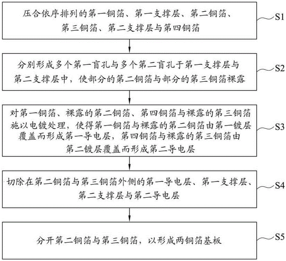
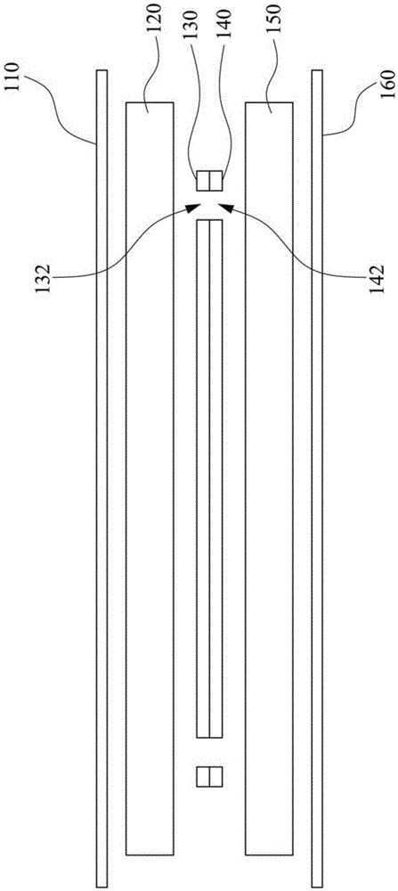
[0049] figure 1 A flowchart illustrating a method for manufacturing a copper foil substrate according to an embodiment of the present invention. The manufacturing method of the copper foil substrate includes the following steps. Firstly, in step S1, the first copper foil, the first support layer, the second copper foil, the third copper foil, the second support layer and the fourth copper foil arranged...


PUM


Abstract

The invention discloses a copper foil substrate manufacturing method. The copper foil substrate manufacturing method comprises the steps of: laminating first copper foil, a first supporting layer, second copper foil, third copper foil, a second supporting layer and fourth copper foil; forming a plurality of first blind holes in the first supporting layer, and forming a plurality of second blind holes in the second supporting layer, so that part of the second copper foil and part of the third copper foil are exposed; carrying out electroplating treatment on the first copper foil, the exposed second copper foil, the fourth copper foil and the exposed third copper foil, so that the first copper foil and the exposed second copper foil are covered by a first plating layer to form a first conductive layer, and the fourth copper foil and the exposed third copper foil are covered by a second plating layer to form a second conductive layer; cutting off the first conductive layer, the first supporting layer, the second supporting layer and the second conductive layer on the outer sides of the second copper foil and the third copper foil; and separating the second copper foil from the third copper foil.

Description

technical field [0001] The invention relates to a manufacturing method of a copper foil substrate. Background technique [0002] HDI (High Density Interconnect) is a high-density interconnection technology, which is one of the technologies used in printed circuit boards (Printed circuit board). HDI circuit boards are mainly made with the technology of blind holes and buried holes. HDI circuit boards are characterized by high-density circuit distribution, but due to the increase in circuit density, HDI circuit boards cannot use traditional drilling methods to form holes, but non-mechanical drilling processes must be used. HDI circuit boards can be applied to electronic products such as smart phones, notebook computers, tablet computers, digital cameras, automotive electronics, and digital cameras. [0003] The development trend of HDI circuit boards is to develop in a thinner and thinner direction. When thin substrates are used more and more frequently, if the HDI circuit ...

Claims


Application Information

Patent Timeline
IPC IPC(8): H05K3/00
CPCH05K3/0097
Inventor 杨伟雄杨中贤孙奇杨婧
Owner TRIPOD WUXI ELECTRONICS
Why Eureka
Try Eureka