Method of coating PCB with solder paste

A kind of PCB board and solder paste technology, applied in the direction of metallurgical bonding, assembling printed circuits with electrical components, etc., can solve the problems of difficult to accurately control the thickness of immersion tin, reduce product competitiveness, product reliability problems, etc., to improve the semi-finished products of PCB boards. Yield, get rid of the dependence of employee skills, improve the effect of finished product yield

Inactive Publication Date: 2017-04-26
SHENZHEN SUCCESS ELECTRONICS LTD +3
View PDF3 Cites 6 Cited by
  • Summary
  • Abstract
  • Description
  • Claims
  • Application Information

AI Technical Summary

Problems solved by technology

Due to the operation proficiency of the staff and the problem of hot air pressure, it is difficult to accurately control the thickness of the dipped tin, and the abnormal tin thickness after dipping will lead to poor soldering of the module tin pressing

Method used


Image

  • Method of coating PCB with solder paste

Examples


Embodiment Construction

[0013] The present invention will be described in further detail below through specific embodiments and in conjunction with the accompanying drawings.

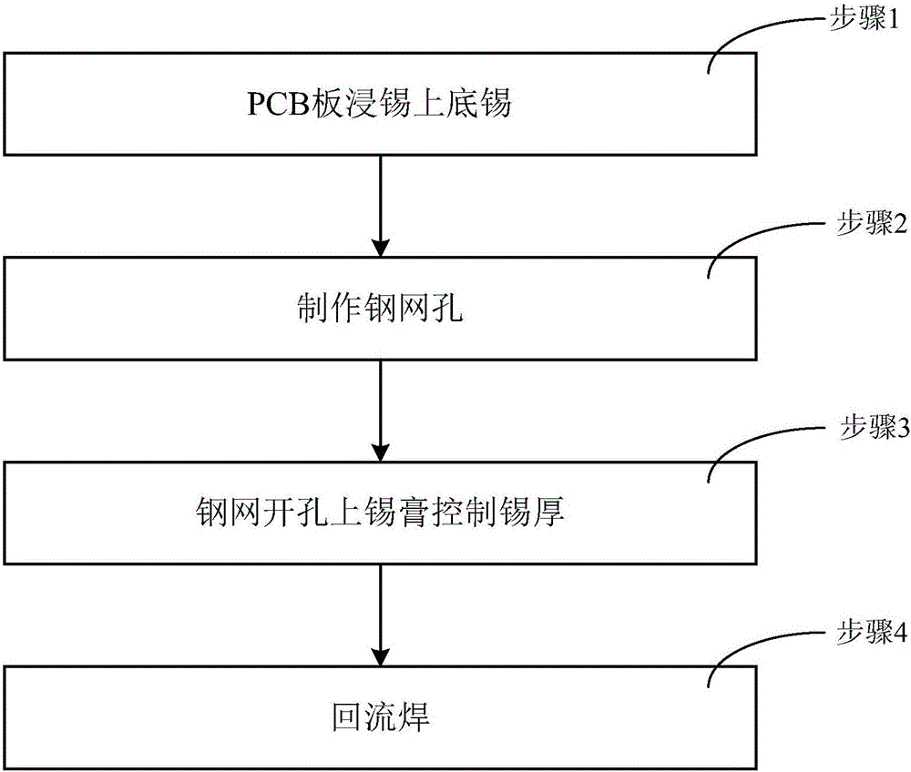
[0014] Such as figure 1 As shown, a method for solder paste on a PCB described in the embodiment of the present invention, the method specifically includes:

[0015] Step 1. After the PCB pads or through-holes are printed, add a layer of bottom tin on the pads or through-hole rings corresponding to the positions to be soldered by dipping tin in a tin furnace;

[0016] Step 2, making a stencil, and the openings on the stencil correspond to the pads or through holes on the PCB;

[0017] Step 3, apply solder paste on the stencil, and pour the solder paste on the stencil into the holes of the stencil corresponding to the solder pads or through holes on the PCB through the balanced movement of the scraper;

[0018] Step 4, separating the stencil from the PCB after performing reflow soldering on the PCB with a tin press.

[0019]...


PUM


Abstract

The invention discloses a method of coating a PCB with solder paste. The method concretely includes the following steps: after printing of a pad or through hole of a PCB is finished, adding a layer of bottom tin on the pad or the ring of the through hole corresponding to a place that needs welding through tin immersion of a tin furnace; making a steel mesh, wherein holes in the steel mesh correspond to the pad or the through hole of the PCB; coating the steel mesh with solder paste, making a scraper move in a balanced manner to fill the holes in the steel mesh, corresponding to the pad or the through hole of the PCB, with the solder paste on the steel mesh; and separating the steel mesh with the PCB after reflow soldering is carried out by a tin press for the PCB. The beneficial effects are that the thickness of tin needs not to be controlled during tin immersion of the PCB, the holes are disposed in the steel mesh and filled with the solder paste during a SMT process when the PCB is coated with the bottom tin so that the thickness of tin is controlled, the cost is not added, the quality is reliable, management and control is convenient, the yield rate of a finished product is greatly improved, and the method can be independent of skills of employees; and after solder paste is disposed in welding positions, standards for the thickness of tin immersion can be loose, and the yield rate of a PCB semi-finished product can be increased.

Description

technical field [0001] The invention relates to a method for solder paste on a PCB. Background technique [0002] In FOG technology, PCB is completed by tin pressing process in the manufacturing process, and the quality and reliability of tin pressing are directly related to the tin thickness of PCB board. In the traditional PCB board manufacturing process, the bottom tin of the soldering position is completed by dipping tin in a tin furnace, and the thickness control of the tin after dipping is obtained by the speed of personnel picking up and the pressure of hot air. Due to the operation proficiency of the staff and the problem of hot air pressure, it is difficult to accurately control the thickness of the dipped tin, and the abnormal tin thickness after dipping will lead to poor soldering of the module tin pressing process, which in turn leads to product reliability problems Leading to customer complaints, product returns and rework and related claims, greatly increasing...

Claims


Application Information

Patent Timeline
IPC IPC(8): H05K3/34
CPCH05K3/34H05K2203/04
Inventor 卢键陈洪发吴晓丽杨慧
Owner SHENZHEN SUCCESS ELECTRONICS LTD
Why Eureka
Try Eureka