Optoelectronic component and method for producing same

A technology for optoelectronic devices and structures, applied in semiconductor/solid-state device manufacturing, electrical solid-state devices, electrical components, etc., can solve the problems of inability to be directly electrically contacted, reduce the active area of ​​optoelectronic devices, and unfavorable production costs, and improve efficiency. , The effect of improving mechanical stability and low contact resistance

Active Publication Date: 2017-05-10
OSRAM OLED
View PDF5 Cites 2 Cited by
  • Summary
  • Abstract
  • Description
  • Claims
  • Application Information

AI Technical Summary

Problems solved by technology

[0007] Conventional optoelectronic devices also have the disadvantage that they cannot be directly electrically contacted after their manufacture due to their electrically insulating thin-film encapsulation deposited over their entire surface
An optoelectronic inspection of the function of the optoelectronic component as quickly as possible in the production method is therefore disadvantageously not possible
The optoelectronic failure of the optoelectronic component is thus processed further in an unknown manner after its production, which disadvantageously results in additional production costs
[0008] In addition, the contact areas usually used for external electrical connections reduce the active area of ​​the optoelectronic component proportionally and disadvantageously prevent a frameless arrangement of several optoelectronic components side by side laterally to form an optoelectronic component

Method used


Image

  • Optoelectronic component and method for producing same
  • Optoelectronic component and method for producing same
  • Optoelectronic component and method for producing same

Examples


Embodiment Construction

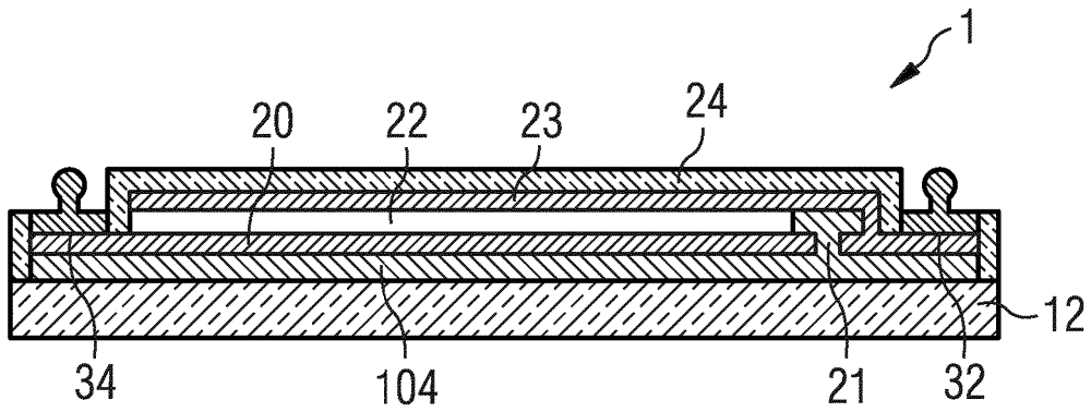
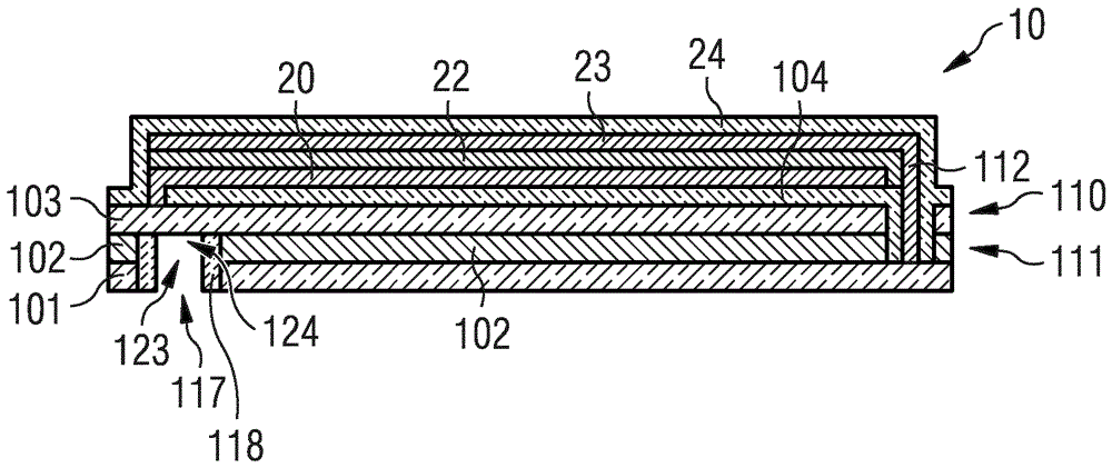
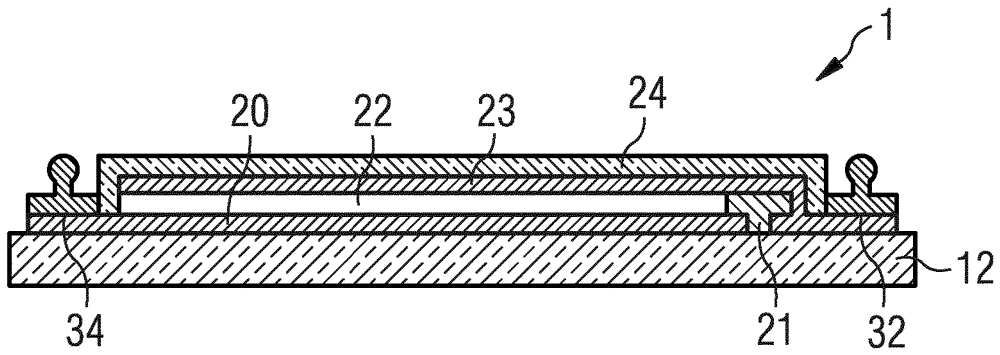
[0063]In the ensuing detailed description, reference is made to the accompanying drawings, which form a part of this specification and in which, for the sake of illustration, specific exemplary embodiments are shown in which the invention can be implemented. In this regard, directional terms such as "upper", "lower", "front", "rear", "front", "rear", etc. are used with reference to the orientation of the figures being described. Because components of an embodiment may be positioned in a number of different orientations, directional terms are used for clarity and are not limiting in any way. It is to be readily understood that different embodiments may be utilized and structural or logical changes may be made without departing from the scope of the present invention. It is easy to understand that the features of different embodiments described herein can be combined with each other unless otherwise specified. The following detailed description should therefore not be read in a...


PUM


Abstract

An optoelectronic component (10) and a method for producing same are provided in various exemplary embodiments. The optoelectronic component (10) has a first electrically conductive contact layer (101), an electrically insulating layer (102) over the first electrically conductive contact layer (101), a second electrically conductive contact layer (103) over the electrically insulating layer (102), a first electrically conductive electrode layer (20) over the second electrically conductive contact layer (103), at least one optically functional layer structure (22) over the first electrically conductive electrode layer (20) and a second electrically conductive electrode layer (23) over the optically functional layer structure (22). The second electrically conductive contact layer (103) comprises a first recess (110). The electrically insulating layer (102) comprises a second recess (111) which overlaps the first recess (110). An electrically conductive through-contact (112) is arranged in the first recess (110) and in the second recess (111), said through-contact being guided to the first electrically conductive contact layer (101). The electrically conductive through-contact (112) is electrically insulated with respect to the second electrically conductive contact layer (103).

Description

technical field [0001] The invention relates to an optoelectronic component having at least one optically functional layer structure and a method for producing such an optoelectronic component. Background technique [0002] The light-emitting optoelectronic component may be, for example, a light-emitting diode (LED) or an organic light-emitting diode (OLED). OLEDs can have an anode and a cathode with an organic functional layer system between them. Organic functional layer systems can have one or more emitter layers (where electromagnetic radiation is generated), respectively two or more carrier pair generation layers for carrier pair generation ("charge generation layers", CGL ), and one or more electron blocking layers, also known as hole transport layers ("hole transport layer" - HTL), and one or more hole blocking layers, Also known as the electron transport layer ("electron transport layer" - ETL) in order to regulate the passing current. [0003] Organic functional ...

Claims


Application Information

Patent Timeline
Patent Type & Authority Applications(China)
IPC IPC(8): H01L51/52
CPCH10K50/814H10K50/824H10K71/70H10K71/00H10K50/844H10K50/854
Inventor E.赫夫林S.席克坦茨
Owner OSRAM OLED
Why Eureka
Try Eureka