Array substrate, display panel and display device

A technology for array substrates and substrate substrates, which is applied to instruments, semiconductor devices, electrical components, etc., can solve the problems of inability to obtain stable exposure, the influence of pixel aperture ratio, and poor exposure process, so as to improve the production success rate and increase exposure. Stability, the effect of increased exposure

Active Publication Date: 2017-05-17
XIAMEN TIANMA MICRO ELECTRONICS
View PDF18 Cites 31 Cited by
  • Summary
  • Abstract
  • Description
  • Claims
  • Application Information

AI Technical Summary

Problems solved by technology

[0004] However, with the continuous improvement of the PPI of the display panel, the pixel arrangement is getting closer and closer, and the size of each sub-pixel is getting smaller and smaller, which not only brings great challenges to the device design of the display panel, but also causes many headaches. For example, the pixel aperture ratio becomes a bottleneck due to the influence of the process on the line width and line spacing requirements; or in the exposure process, because the distance between the graphics to be formed in adjacent sub-pixels is getting smaller and smaller, The amount of exposure between graphics becomes less and less, and stable exposure cannot be obtained, resulting in poor exposure process and poor display panel

Method used


Image

  • Array substrate, display panel and display device
  • Array substrate, display panel and display device
  • Array substrate, display panel and display device

Examples


Embodiment Construction

[0040] The following will clearly and completely describe the technical solutions in the embodiments of the present invention with reference to the accompanying drawings in the embodiments of the present invention. Obviously, the described embodiments are only some, not all, embodiments of the present invention. Based on the embodiments of the present invention, all other embodiments obtained by persons of ordinary skill in the art without creative efforts fall within the protection scope of the present invention.

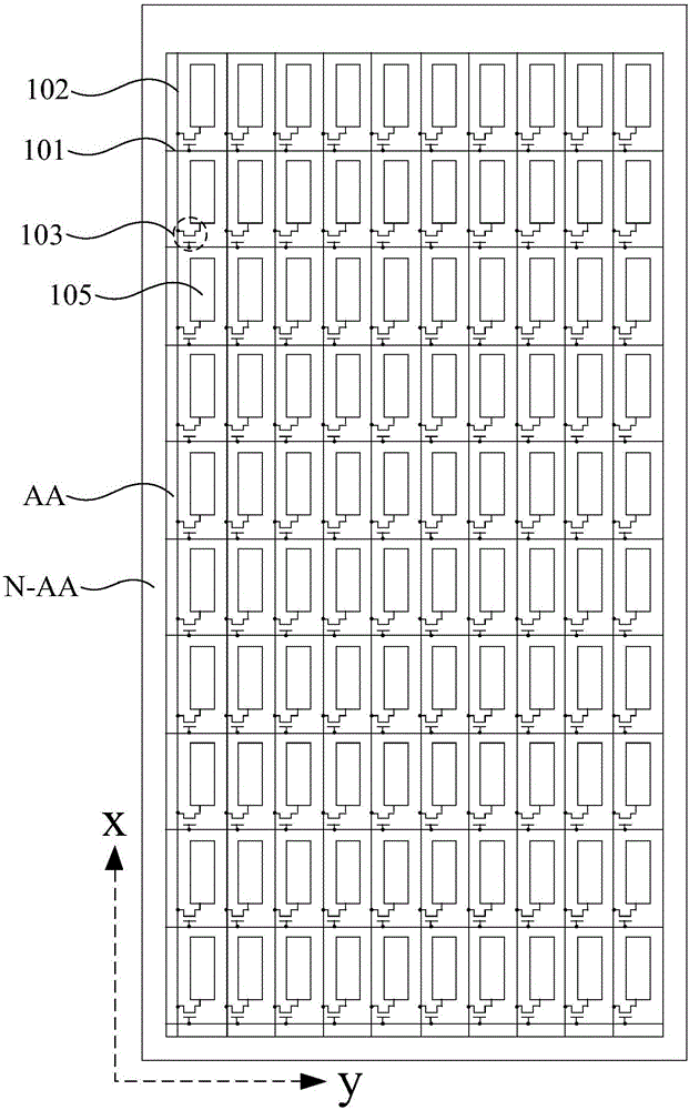
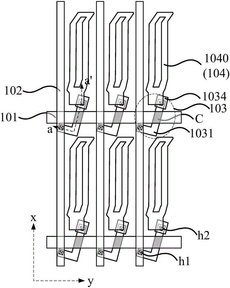
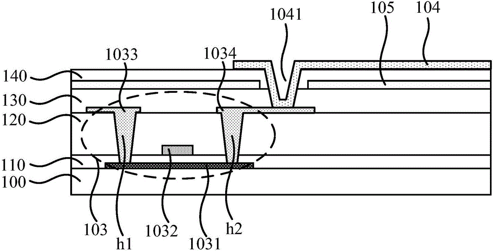
[0041] An embodiment of the present invention provides an array substrate, including a base substrate, a plurality of scanning lines and a plurality of data lines located on one side of the base substrate, the plurality of scanning lines are arranged side by side along a first direction, the A plurality of data lines are arranged side by side along the second direction, and the plurality of scanning lines and the plurality of data lines are insulated and intersect t...


PUM


Abstract

The invention discloses an array substrate, a display panel and a display device. The array substrate comprises an underlayer substrate, multiple scanning lines and multiple data lines. The scanning lines and the data lines are located on one side of the underlayer substrate. The scanning lines are arranged side by side in the first direction, the data lines are arranged side by side in the second direction, and multiple sub-pixels are defined by the scanning lines and the data lines in an insulating cross mode. The sub-pixels comprise thin film transistors, and each thin film transistor comprises an active layer, a grid, a source electrode and a drain electrode which are located on one side of the underlayer substrate. The active layers comprise channel regions, and the regions where the active layers and the grids are overlapped are the channel regions in the direction vertical to the array substrate. Each channel region comprises two opposite edges in the second direction, first included angles are formed between the stretching directions of the edges and the first direction, and the first included angles are larger than 0 degree and smaller than or equal to 40 degrees. The exposure stability of graphs in the thin film transistors can be improved, and the aperture ratio is increased to a certain degree.

Description

technical field [0001] The present invention relates to the field of display technology, in particular to an array substrate, a display panel including the array substrate, and a display device including the display panel. Background technique [0002] Liquid crystal display devices have the advantages of no radiation, thinness, and power saving, and have been widely used in various information, communication, and consumer electronics products. A liquid crystal display device generally includes a display panel, and the display panel includes an array substrate and a color filter substrate disposed opposite to each other, and a liquid crystal layer disposed between the two substrates. The array substrate includes scanning lines and data lines, which are insulated and intersect with each other to define a plurality of sub-pixels; each sub-pixel includes a pixel electrode, a common electrode and a thin film transistor, and the pixel electrode is electrically connected to the dr...

Claims


Application Information

Patent Timeline
Patent Type & Authority Applications(China)
IPC IPC(8): H01L27/12H01L29/10G02F1/1333
CPCG02F1/1333H01L27/1222H01L29/1033G02F1/133707G02F1/134363G02F2201/124G02F1/1368G02F1/136286G02F1/136209G02F2201/123G02F2201/121G02F2201/122G02F1/134309G02F1/13685G02F1/134345G02F1/134372
Inventor 张磊
Owner XIAMEN TIANMA MICRO ELECTRONICS
Why Eureka
Try Eureka