MEMS sensor low stress package and package system

A technology for packaging systems and packaging tubes, which is applied to parts, instruments, and measuring devices of TV systems, and can solve problems such as the back layer of MEMS chips not being too thick, the ability to resist mechanical shock, and the strength of soft adhesive sheets are not enough. Achieve the effects of reducing package stress, high thermal conductivity, and increasing accuracy

Inactive Publication Date: 2017-05-31
INST OF GEOLOGY & GEOPHYSICS CHINESE ACAD OF SCI
View PDF10 Cites 22 Cited by
  • Summary
  • Abstract
  • Description
  • Claims
  • Application Information

AI Technical Summary

Problems solved by technology

However, since MEMS chips generally use standard MEMS wafer materials and equipment, and MEMS chips are generally small in size, the back layer of MEMS chips should not be too thick; When the stress is released, the packaging stress from the package shell is effectively isolated. However, the soft adhesive is generally an organic material,

Method used


Image

  • MEMS sensor low stress package and package system
  • MEMS sensor low stress package and package system
  • MEMS sensor low stress package and package system

Examples


Embodiment Construction

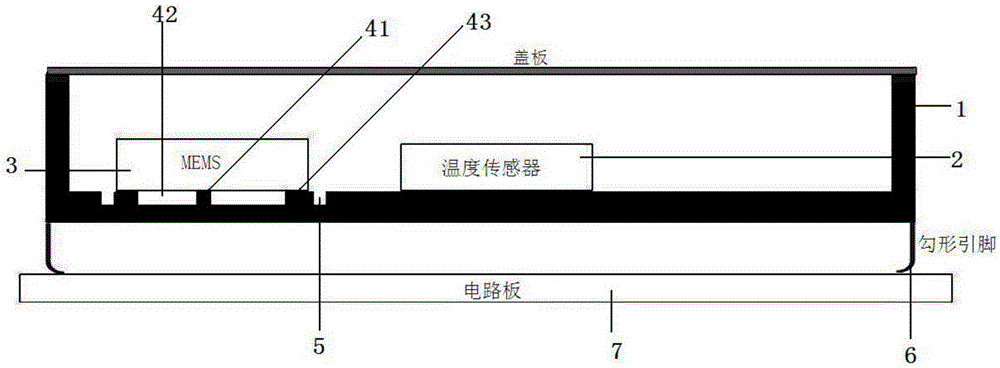
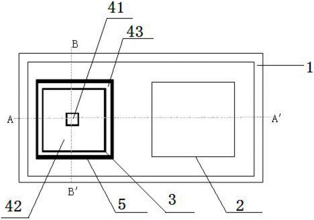
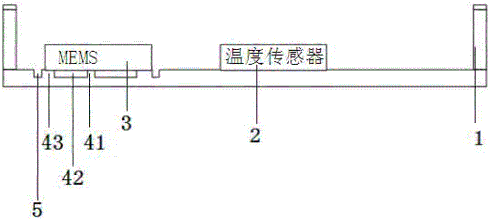
[0026] In order to make the object, technical solution and advantages of the present invention clearer, the present invention will be further described in detail below in conjunction with the accompanying drawings and embodiments. It should be understood that the specific embodiments described here are only used to explain the present invention, not to limit the present invention. On the contrary, the invention covers any alternatives, modifications, equivalent methods and schemes within the spirit and scope of the invention as defined by the claims. Further, in order to make the public have a better understanding of the present invention, some specific details are described in detail in the detailed description of the present invention below. The present invention can be fully understood by those skilled in the art without the description of these detailed parts.

[0027] The present invention will be further described below in conjunction with the accompanying drawings and ...


PUM


Abstract

The invention provides an MEMS sensor low stress package and a package system. An islet structure and a stress isolation groove are arranged inside the bottom of the package. The bottom of the package is provided with the islet structure and the stress isolation groove. The stress isolation groove is applied to isolate the effect which is imposed on a MEMS chip by the package deformation and to ensure the stability of a paster area of the MEMS chip. The location and area of the dispensing islet are changed according to different chips. The texture of the package is aluminum nitride. Because a hooked pin has the effect of supporting and delivering electrical signal, the hooked pin is capable of isolating the effect on the package caused by self-deformation of a circuit board and is capable of isolating the package and the circuit board. When the temperature is changed, the package and the circuit board are not contacted with each other to produce the stress. On one hand, the stress isolation groove isolates the stress from the package and makes the stress not conducted to MEMS chip. On the other hand, because of making most area of the MEMS chip not contacted with the package, the stress produced by thermal expansion mismatch is avoided.

Description

technical field [0001] The invention belongs to the field of micro-electromechanical systems, and in particular relates to a low-stress packaging system for MEMS sensors. Background technique [0002] Electronic packaging is to electrically connect one or more electronic component chips to each other, and then encapsulate them in a protective structure. Its purpose is to provide electrical connection, mechanical protection, chemical corrosion protection, etc. for electronic chips. For some electronic products, such as gyroscopes, accelerometers, oscillators, or bulk acoustic wave filters in MEMS devices, are very sensitive to stress, it is necessary to use ceramic shells, metal shells, or preformed plastic shells to protect MEMS chips. Hermetically sealed. The traditional packaging structure is to apply adhesive on the bottom plate of the package shell, load the MEMS chip, and fix the back layer of the MEMS chip on the bottom plate of the package shell through the adhesive,...

Claims


Application Information

Patent Timeline
IPC IPC(8): B81B7/00B81B7/02
CPCB81B7/0032B81B7/0048B81B7/02B81B2207/09
Inventor 郭士超薛旭
Owner INST OF GEOLOGY & GEOPHYSICS CHINESE ACAD OF SCI
Why Eureka
Try Eureka