Broad-band high-diffraction-efficiency asymmetric morphology reflection grating
A diffraction-efficient, asymmetric technology, applied in the directions of diffraction gratings, optics, optical components, etc., to achieve the effect of simple grating structure
- Summary
- Abstract
- Description
- Claims
- Application Information
AI Technical Summary
Problems solved by technology
Method used
Image


Examples
Embodiment 1
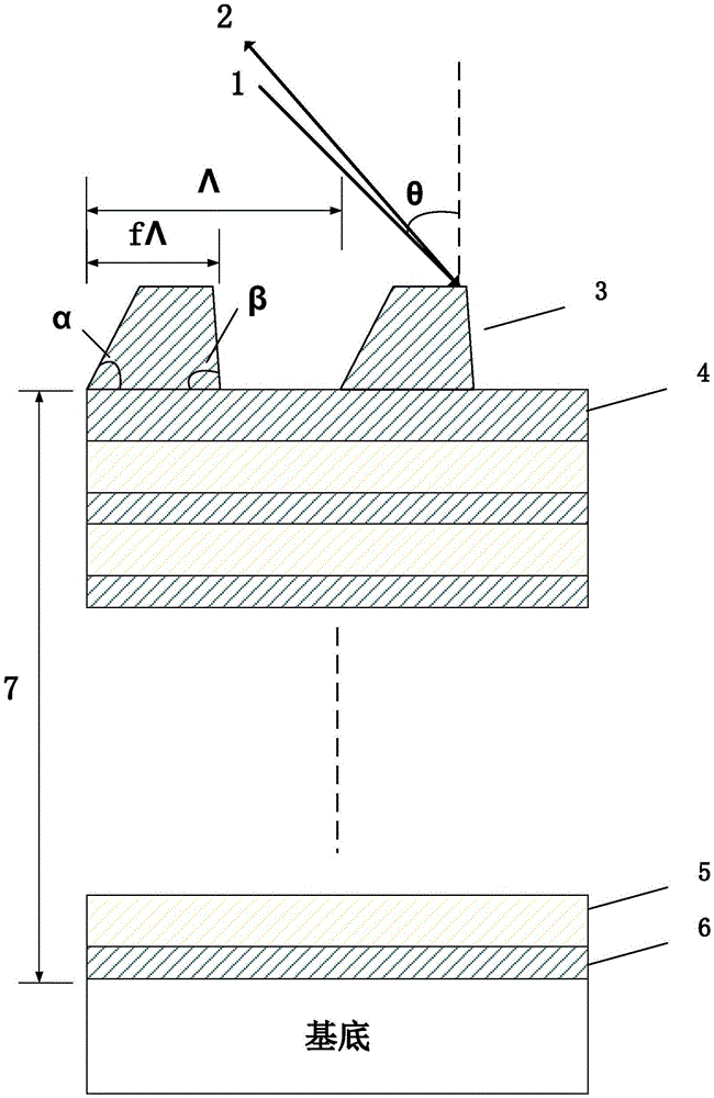
[0029] Broadband high diffraction efficiency asymmetric topography reflective gratings, such as figure 1 As shown, the grating consists of a top grating ridge structure 3, a middle high-reflectivity film layer 7 and a bottom substrate. The top grating ridge structure has an asymmetric shape, and the corresponding bottom angles α and β are 68° and 89°. The film structure of the grating is S|(HL) 15 RG|A, where S represents the substrate, H represents the high refractive index film layer 6 (Ta 2 o 5 ), L represents the low refractive index film layer 5 (SiO 2 ), the film period is 15 periods, and R represents the remaining dielectric layer of the grating with a thickness of 256 nm (HfO 2 ), G represents the grating ridge structure layer with a height of 400 nm (HfO 2 ), A means air. The period of the grating is 833 nanometers, the corresponding grating line density is 1200 lines per millimeter, and the bottom occupation ratio f is 0.66. Such as image 3 As shown, when th...
Embodiment 2
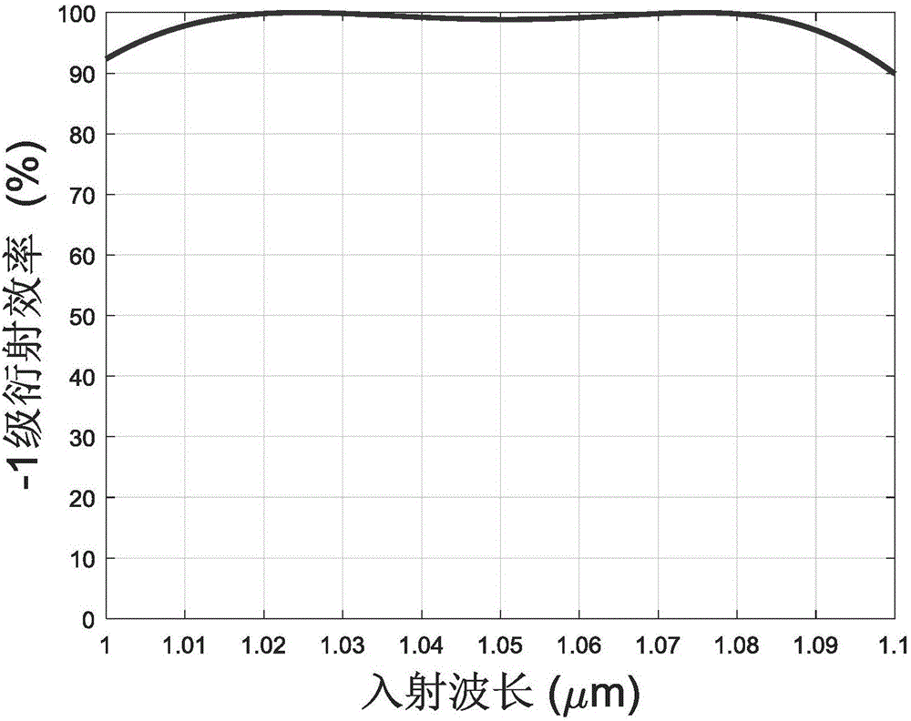
[0031] Broadband high diffraction efficiency asymmetric topography reflective gratings, such as figure 2 As shown, the grating structure is composed of the top grating ridge structure 3, the middle high-reflectivity film layer 7 and the bottom substrate, wherein the top grating ridge structure has an asymmetric shape, and the corresponding base angles α and β are 68° and 89° respectively . The film structure of the grating is S|MRG|A, where S represents the substrate, M represents the high-reflectivity metal layer (Au) with a thickness of 200 nm, and R represents the remaining dielectric layer (HfO) with a thickness of 168 nm. 2 ), G represents the grating ridge structure layer with a height of 567 nm (HfO 2 ), A means air. The period of the grating is 683 nanometers, the corresponding grating line density is 1464 lines per millimeter, and the grating duty ratio is 0.6. Such as Figure 5 It is shown that when the incident light is incident at the Littrow angle, in the ran...
PUM
 Abstract
Description
Claims
Application Information
 - Generate Ideas
- Intellectual Property
- Life Sciences
- Materials
- Tech Scout
- Unparalleled Data Quality
- Higher Quality Content
- 60% Fewer Hallucinations
Browse by: Latest US Patents, China's latest patents, Technical Efficacy Thesaurus, Application Domain, Technology Topic, Popular Technical Reports.
© 2025 PatSnap. All rights reserved.Legal|Privacy policy|Modern Slavery Act Transparency Statement|Sitemap|About US| Contact US: help@patsnap.com