Broadband polarization-independent long-wave infrared absorber plate
A long-wave infrared, absorption plate technology, applied in instruments, optics, filters, etc., can solve the problem that infrared absorbers cannot take into account the absorption rate, absorption bandwidth and duty cycle.
- Summary
- Abstract
- Description
- Claims
- Application Information
AI Technical Summary
Problems solved by technology
Method used
Image
Examples
Embodiment 1
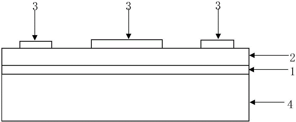
[0048] Embodiment 1: asfigure 1 As shown, this embodiment includes a substrate layer 4, a bottom metal layer 1, a dielectric layer 2 and a top metal layer 3 from bottom to top, and the bottom metal layer is a continuous metal layer;
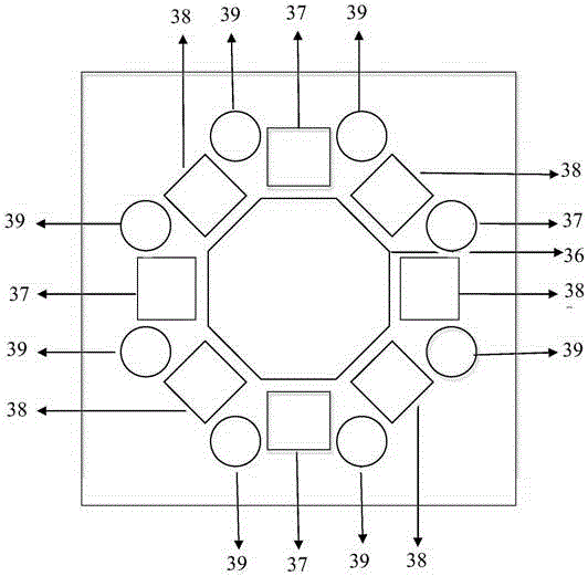
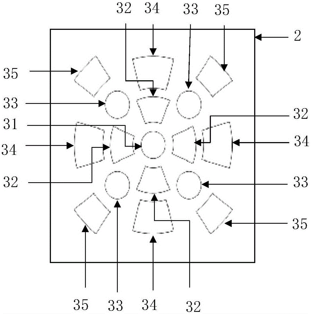
[0049] The top metal layer 3 is composed of a plurality of metal pattern groups arranged in a periodic array. Each metal pattern group has the same structure and is composed of a plurality of symmetrically arranged metal pattern units. The size of each metal pattern unit is similar. The metal graphic unit together with the dielectric layer and the underlying metal layer under its vertical projection form a resonant unit, and the thickness of the dielectric layer is adjusted so that the impedance of each resonant unit matches the impedance of the external environment;
[0050] The substrate layer 4 is made of silicon material;
[0051] The bottom metal layer 1 and the top metal layer 3 are made of gold material with a thickness of 100 nanometers; ...
Embodiment 2
[0061] Embodiment 2: as Figure 4 As shown, this embodiment includes a substrate layer 4, a bottom metal layer 1, a dielectric layer 2 and a top metal layer 3 from bottom to top, and the bottom metal layer is a continuous metal layer;
[0062] The top metal layer 3 is composed of a plurality of metal pattern groups arranged in a periodic array. Each metal pattern group has the same structure and is composed of a plurality of symmetrically arranged metal pattern units. The size of each metal pattern unit is similar. The metal graphic unit together with the dielectric layer and the underlying metal layer under its vertical projection form a resonant unit, and the thickness of the dielectric layer is adjusted so that the impedance of each resonant unit matches the impedance of the external environment;
[0063] The dielectric layer 2 has the same pattern as the vertical projection of the top metal layer 3, and coincides with the pattern of the top metal layer 3 in the vertical di...
PUM
| Property | Measurement | Unit |
|---|---|---|
| Diameter | aaaaa | aaaaa |
| Diameter | aaaaa | aaaaa |
| Diameter | aaaaa | aaaaa |
Abstract
Description
Claims
Application Information


