Optical module

A technology of optical module and optical chip, which is applied in the field of optical communication, can solve problems such as performance defects and EMC performance of equipment that cannot meet the specified requirements, and achieve the effect of improving EMC performance and reducing electromagnetic radiation

Active Publication Date: 2017-05-31
HISENSE BROADBAND MULTIMEDIA TECH
View PDF5 Cites 10 Cited by
  • Summary
  • Abstract
  • Description
  • Claims
  • Application Information

AI Technical Summary

Problems solved by technology

[0005] see Figure 4 , since the high-speed signal lines 223a and 225a are in the form of microstrip lines, such microstrip lines will generate relatively large outward electromagnetic radiation when carrying high frequency, large voltage swing, and large current swing, and this electromagnetic radiation will Radiation through the port of the optical module 10a causes certain defects in the EMC (Electro Magnetic Compatibility, electromagnetic compatibility) performance of the optical module 10a, which in turn will cause the EMC performance of the device equipped with the optical module 10a to fail to meet the specified requirements

Method used


Image

  • Optical module
  • Optical module
  • Optical module

Examples


Embodiment Construction

[0024] The present invention will be further elaborated below in conjunction with the accompanying drawings.

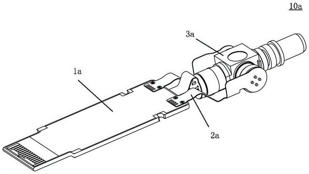
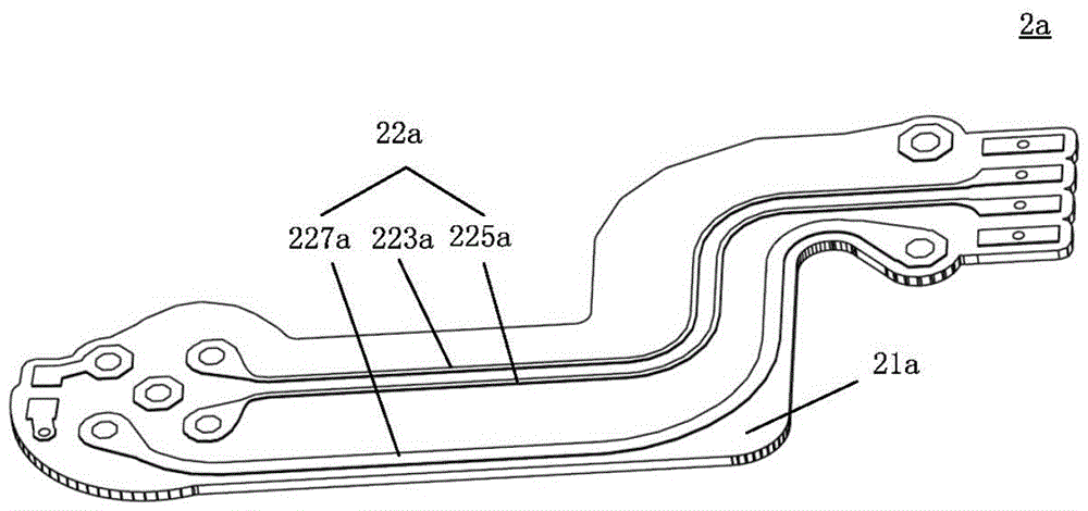
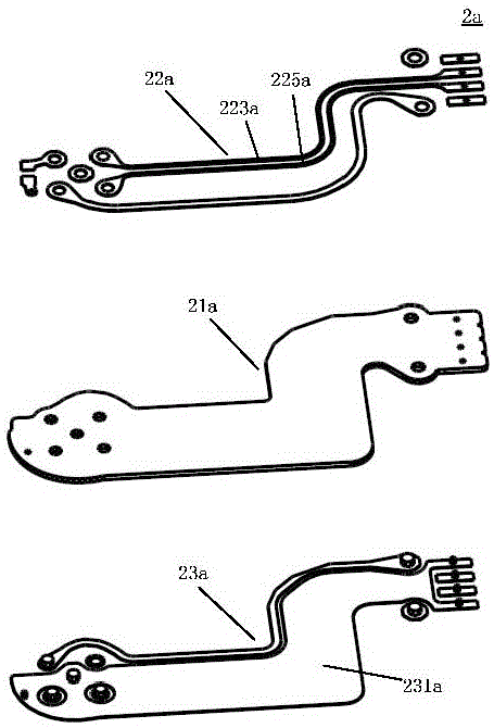
[0025] see figure 1 , the circuit board in the optical module 10a includes a flexible circuit board 2a and a rigid circuit board 1a. The optical module includes an optical chip and an optical chip driver chip. For example, the optical chip is a laser, and its driver chip is a device used to provide transmission signal processing; another example: the optical chip is a detector, and its driver chip is used to provide transmission signal processing. The optical chip can be located on a flexible circuit board or a hard circuit board; the optical chip driver chip can be located on a flexible circuit board or a hard circuit board.

[0026] In high-speed optical modules, high-speed signals are transmitted on the circuit board, such as 25G and 100G rates. High-speed signal lines will generate high electromagnetic radiation, which will affect the normal operation of other el...


PUM


Abstract

The invention provides an optical module for solving technical problems. The technical scheme includes that the optical module comprises a circuit board, an optical chip and an optical-chip driving chip; an upper and lower metal mesh layers are arranged on the circuit board, and the metal mesh layers are grounded; a high-speed signal line is sandwiched between the metal mesh layers, and the optical chip and the optical-chip driving chip are electrically connected through the high-speed signal line; multiple metal overholes communicated with the metal mesh layers are arranged around the high-speed signal line, and the metal mesh layers and the metal overholes form a shield cage to have the high-speed signal line shielded. Two ground planes and the metal overholes are ingeniously arranged on the circuit board to form the shield cage to have the high-speed signal line shielded, leakage of electromagnetic radiation of the high-speed signal line to the outside of the circuit board can be greatly reduced, and EMC (electro-magnetic compatibility) of the optical module can be effectively improved.

Description

technical field [0001] The invention relates to the field of optical communication, in particular to an optical module. Background technique [0002] see figure 1 , the flexible circuit board 2a on the optical module 10a is responsible for connecting the rigid circuit board 1a and the optical sub-module 3a. The optical sub-module 3a can be ROSA (Receiving Optical Sub-Assembly, light receiving assembly), TOSA (Transmitting Optical Sub-Assembly, light emitting assembly) or BOSA (Bi-Directional Optical Sub-Assembly, light transmitting and receiving assembly). The optical module includes an optical chip and an optical chip driver chip. For example, the optical chip is a laser, and its driver chip is a device used to provide transmission signal processing; another example: the optical chip is a detector, and its driver chip is used to provide transmission signal processing. device. [0003] With the continuous improvement of optical communication data transmission, the data ra...

Claims


Application Information

Patent Timeline
Patent Type & Authority Applications(China)
IPC IPC(8): G02B6/42
CPCG02B6/4277G02B6/428
Inventor 赵伟于冬梅
Owner HISENSE BROADBAND MULTIMEDIA TECH
Why Eureka
Try Eureka