Array substrate and its manufacturing method and In Cell touch control display panel

A touch display panel and array substrate technology, applied in optics, instruments, electrical digital data processing, etc., can solve the problems affecting the display quality of the panel, changes in the thickness of the liquid crystal cell, scratches on the alignment film, etc., so as to improve the display quality, surface The effect of flatness and process cost reduction

Inactive Publication Date: 2017-05-31
WUHAN CHINA STAR OPTOELECTRONICS TECH CO LTD
View PDF6 Cites 11 Cited by
  • Summary
  • Abstract
  • Description
  • Claims
  • Application Information

AI Technical Summary

Problems solved by technology

[0014] It can be seen from the structure of the array substrate 100 and its manufacturing method that since the array substrate 100 contains a total of three passivation layers of the first passivation layer 810, the second passivation layer 820, and the third passivation layer 830, layers, making the manufacturing process complicated and the manufacturing cost higher;
[0015] In addition, since the touch signal layer 600 is relatively thick and is located on the flat layer 500 , the area on the surface of the array substrate 100 corresponding to the touch signal layer 600 will

Method used


Image

  • Array substrate and its manufacturing method and In Cell touch control display panel
  • Array substrate and its manufacturing method and In Cell touch control display panel
  • Array substrate and its manufacturing method and In Cell touch control display panel

Examples


Example Embodiment

[0048] In order to further illustrate the technical means adopted by the present invention and its effects, the following describes in detail in conjunction with preferred embodiments of the present invention and accompanying drawings.

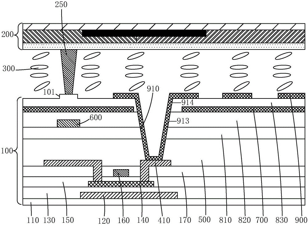
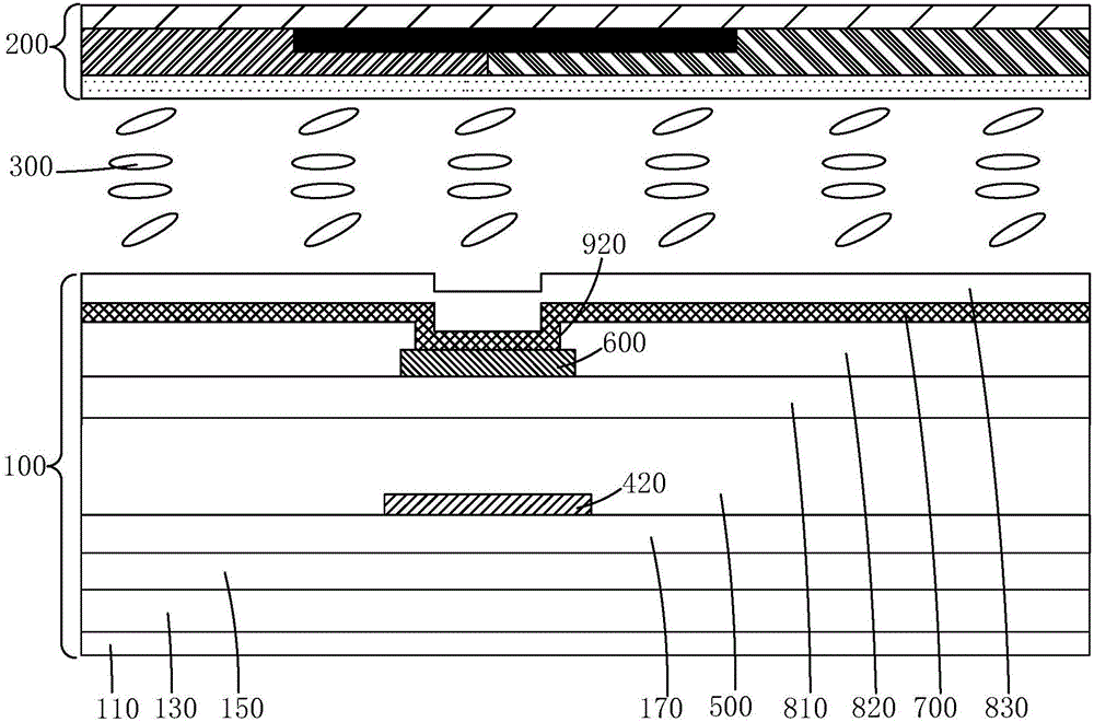
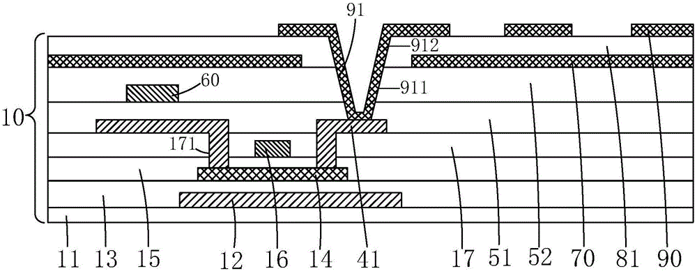
[0049] see image 3 and Figure 4 The present invention firstly provides an array substrate 10, including a first substrate 11, a light-shielding layer 12 disposed on the first substrate 11, and a first insulating layer 13 disposed on the first substrate 11 and the light-shielding layer 12. , the active layer 14 disposed on the first insulating layer 13, the second insulating layer 15 disposed on the first insulating layer 13 and the active layer 14, the second insulating layer 15 disposed on the second insulating layer 15 The gate 16, the third insulating layer 17 disposed on the gate 16 and the second insulating layer 15, the source / drain 41 and the data line 42 disposed on the third insulating layer 17, disposed on the The source / drain el...


PUM


Abstract

The invention provides an array substrate and its manufacturing method and an In Cell touch control display panel. According to the array substrate, a first flat layer, a touch control signal layer, a second flat layer, a common electrode, a passivation layer and a pixel electrode are sequentially formed on a source/drain electrode, a data line and a third insulating layer, in the structure, the touch control signal layer is located below the second flat layer, the situation that bulges form in the region, corresponding to the touch control signal layer, on the surface of the array substrate does not occur, the surface of the array substrate is relatively flat, the situation that sliding of a spacer causes the collapse of a liquid crystal box or the scratch of an alignment film can be avoided, and the displaying quality is improved; at the same time, three passivation layers in an existing array substrate are reduced to one passivation layer, the manufacture procedure is thus simplified, and the manufacturing cost is reduced. According to the manufacturing method of the array substrate, the surface of the prepared array substrate is flat, the manufacture procedure is simple, and the manufacturing cost is low. The In Cell touch control display panel is good in displaying quality and low in production cost.

Description

technical field [0001] The invention relates to the field of display technology, in particular to an array substrate, a manufacturing method thereof, and an In Cell touch display panel. Background technique [0002] With the rapid development of display technology, touch display panels have been widely accepted and used by people, for example, smart phones, tablet computers, etc. all use touch display panels. The touch display panel adopts embedded touch technology to integrate the touch panel and the liquid crystal display panel, and embeds the function of the touch panel into the liquid crystal display panel, so that the liquid crystal display panel has the functions of displaying and sensing touch input at the same time. According to different structures, the touch display panel can be divided into a type in which the touch electrodes are covered on the liquid crystal cell (On Cell), a type in which the touch electrodes are embedded in the liquid crystal cell (In Cell), a...

Claims


Application Information

Patent Timeline
IPC IPC(8): G02F1/1333G02F1/1339G02F1/1335
CPCG02F1/13338G02F1/133514G02F1/13394G02F1/13396G02F1/136209G02F1/136227G06F3/0412G06F2203/04103G02F1/134372G02F1/13685G02F1/133345G02F2202/104G02F1/133357
Inventor 李亚锋
Owner WUHAN CHINA STAR OPTOELECTRONICS TECH CO LTD
Why Eureka
Try Eureka